How to Successfully Design With a BGA

Table of Contents
Currently, the standard packaging for housing a variety of advanced multifunctional semiconductor devices like FPGAs and microprocessors is the Ball Grid Array (BGA). Components in BGA packages are used in a huge range of embedded designs, either as host processors or as peripherals like memories. BGAs have evolved significantly over the years to keep up with technological progression of chip manufacturers, and variations of BGA packages are being used in specialized leadless packaging for a variety of devices. However, in HDI design and layout, the most difficult components to work with are BGAs with high pin count and small pin pitch.
BGA packages can be broken down into standard BGAs and micro BGAs. With today’s electronics technology, the demand for I/O availability poses a number of challenges, even for experienced PCB designers, specifically with regard to routing on multiple layers. What are some strategies we can use to successfully overcome these BGA PCB design challenges?
Starting a PCB Layout With a BGA
Since BGAs are often the main processor in a device, and they may need to interface with many other components in the board, it's common practice to place the largest BGA component first and use it to start floorplanning the PCB layout. While you don't have to place this component first, nor do you need to lock its location once placed, the largest BGA will partially determine the layer count and fanout strategy you'll use to route into the component.
In starting a PCB layout with a BGA, there are a few tasks required to ensure successful routing:
- Signal layer count: Determining the number of signal layers needed in the stackup will influence the number of plane layers, as well the resulting trace width needed to route into the design.
- Fanout: How will signals enter and exit the BGA? Is controlled impedance needed? These questions will determine the layer count in the stackup, which will then determine how traces will be routed in the inner layers.
There is also the matter of design performance and qualification level. High-reliability designs with BGAs will need to perform to Class 3/3A or an even higher product-specific reliability standard. For example, some mil-aero specifications will require pad sizes that will exceed the IPC-6012 Class 3 annular ring requirement. As a result, the standard dog-bone fanout may no longer work due to tolerances, annular ring, and solder mask requirements.
With some of these points in mind earlier in the design process, it's now possible to approach PCB layout with a BGA in three tasks.
BGA Strategy 1: Defining Suitable Exit Routes
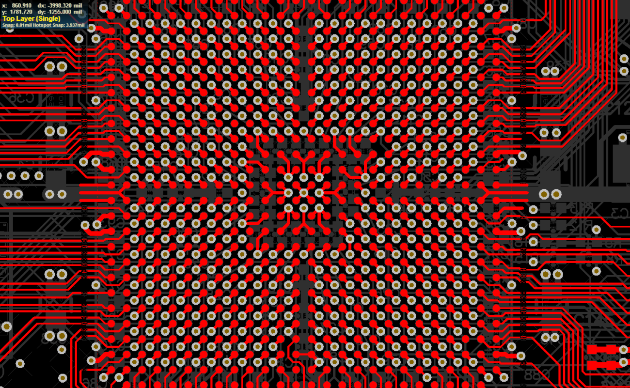
The primary challenge in BGA layout and routing is determining suitable exit routes that can be manufactured reliably and that won’t incur rework of the PCB after assembly. With high layer count BGAs, exit route planning invovles routing traces through multiple rows of pins. Some of these traces may carry high-speed signals, requiring that traces be spaced apart appropriately to prevent crosstalk. Other signals might be slower configuration signals that can be clustered closer together with fewer risks of crosstalk or excessive noise.
The example below shows BGA escape routing on two internal layers. Here, we can see that on these internal layers, the traces are routing into multilpe rows of vias (more than two), which is appropriate given that we are not routing into the surface pins. On the surface, it is most common to only route into the outer two rows due to the pad size in the BGA land pattern, the need for clearances, and the fanout style (specifically dog-bone fanout).

On the top layer, below the BGA, many pads in the land pattern will need to be connected to vias so that connections can be made to internal layers throughout the PCB. For larger-pitch BGAs (up to 1 mm), a dog-bone fanout is the standard method for making these connections. These small traces that connect to vias provide access to the outer two rows of pins on the surface layer (beneath the BGA), and the remaining inner pads through vias from internal layers.
Although dog-bone fanout is the standard method for coarse-pitch BGAs, via-in-pad gives you more flexibility on the surface layer. As pin pitches get smaller, the required trace width needed to reach between pins to a BGA on each layer will get smaller smaller. For controlled impedance signals, this means you will need thinner laminates and, eventually, HDI techniques to ensure you can route into the BGA. The fanout style will eventually change from dog-bone to via-in-pad. To learn more about BGA fanout styles and some alternative breakout methods, we recommend reading the following excellent textbook:
- Pfiel, C. BGA Breakouts and Routing: Effective Design Methods for Very Large BGAs, 2nd Edition. Mentor Graphics (2010).
BGA Design Task 2: Ground and Power
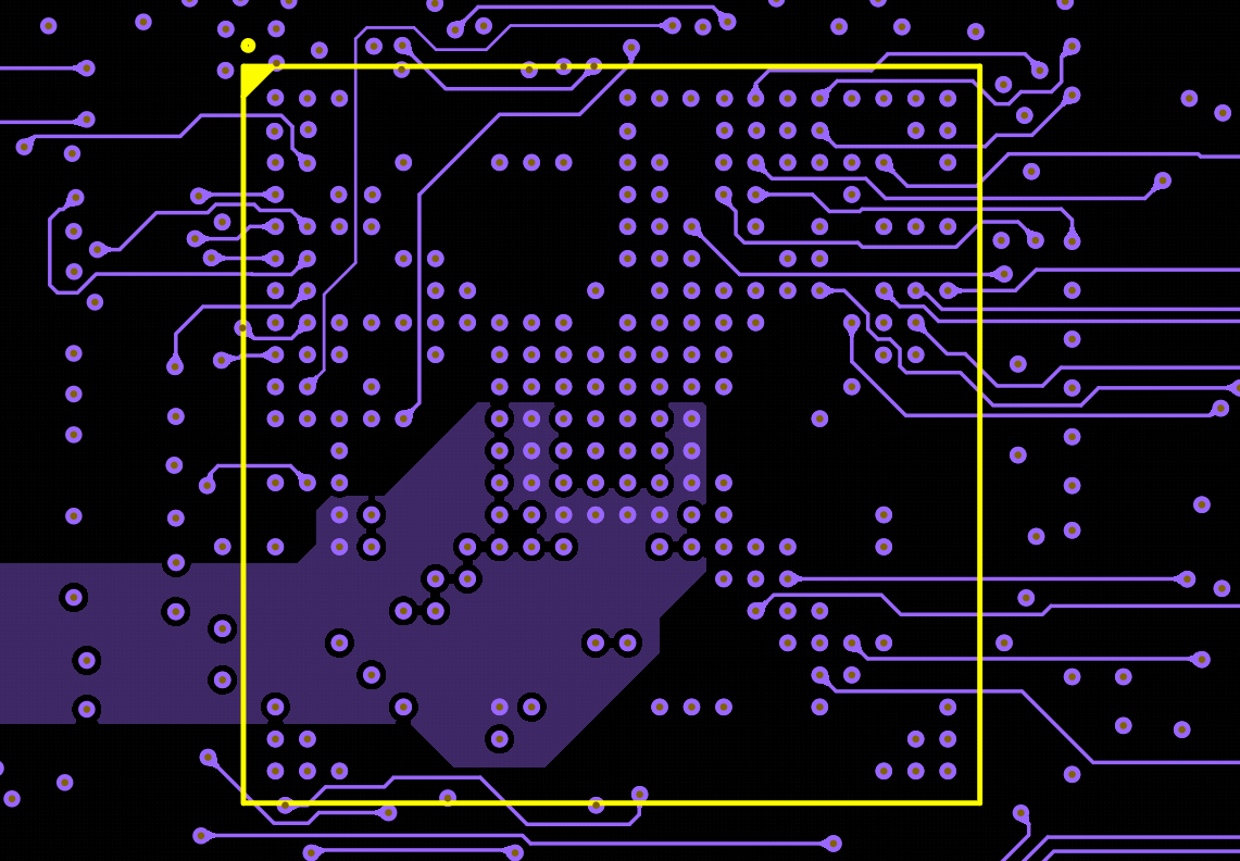
In a large BGA, it's likely that multiple pins will be dedicated to ground and power. In some components, especially large processors that must support multiple high-speed digital interfaces, it's possible the majority of pins can be dedicated to power and ground. In addition, the component could require multiple voltage levels, meaning power from multiple supplies will need to be routed into the board. The easiest way to manage the power connections into a BGA is to use power rails, typically on one or two plane layers. The placement of power and ground on adjacent layers with thin dielectric separation will also help maintain power integrity by providing high interplane capacitance.
Although we always talk about exit routes or escape routing beneath a BGA, this isn't the only type of routing you'll create near your BGA pins. Power rails, connections to ground plane layers or polygons, and routing between pins may all need to be performed beneath the same BGA. This mean that might see routing between pins in addition to polygons for power/ground on the same layer. An example is shown below.
BGA Design Task 3: Determining the PCB Layer Stack
The BGA pinout and I/O count on a BGA can be used to determine the number of layers needed in a PCB stackup. Once a designer has determined the trace width needed to route controlled impedance lines into the BGA, one can determine the layer thickness needed to maintain impedance. Add to this the number of rows in the BGA, and you can now count up the total number of signal layers needed in the PCB stackup.
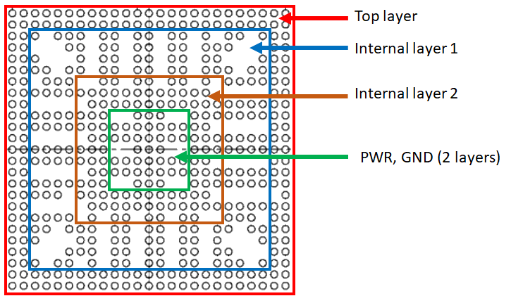
Commonly, the first two outer rows of a BGA device will not require vias, so they can be routed on the surface layer. This would be the case for dog-bone fanouts, via-in-pad, or an alternative fanout. This pattern can then be repeated throughout the BGA to determine the total number of layers needed to fanout signals. It's common that GND pins will be interleaved between signal pins, and GND should be interleaved between signal layers to provide isolation where needed. The graphic below shows how rows can be counted up in a BGA and so that the number of required signal layers can be determined.
In the example below, we show a flip chip BGA with some pins removed from the interior rows. Because some of these balls have been removed, it's possible to route signals there and reach these inner pins, so more than 2 rows might be accessible from the internal layers. The main interior square on this particular BGA could be for power and ground, requiring at least two layers. With these layers and the back layer, the total layer count required to totally fanout and route this BGA would be at least 6 layers.
Learn More BGA Design Strategies For Your PCB
Designing a PCB with a BGA can be difficult, but it starts with setting up your DRC engine to ensure proper routing geometry and spacing is maintained throughout the PCB layout. To learn more about routing BGAs in HDI PCBs, read the resources below:
- Design Basics for HDI and the HDI PCB Manufacturing Process
- Routing High-Density Interconnects with Reliable Microvias
Check out Altium Designer® in action...
Powerful PCB Design
About Author
Related Resources


Related Technical Documentation


Take advantage of the world's
most trusted PCB design system.
One interface. One data
model. Endless possibilities.
Effortlessly collaborate with
mechanical designers.
The world's most trusted
PCB design platform
Best in class interactive
routing
View License Options
Thank you, you are now subscribed to updates.