Defining and Using Multiple Customizable PCB Grids to Save Time on Your Layout Process

Relying on one grid size can require frequent step size changes, as well as a unit of measure change, and possibly even board origin location changes, in order to achieve all required grids. Read to understand how customizable grids can help to resolve this complicated and manual process.
It’s possible to rely exclusively on your default grid for all aspects of component placement, trace routing, and mechanical or special object placement. However, reliance on one grid size requires frequent step size changes, as well as a unit of measure change, and possibly even board origin location changes, in order to achieve all required grids. This is where customizable grids come in to resolve this complicated and manual process.
Using Grids to Speed Up Your Design Process
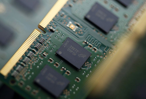
Placing components of a specific grid can help speed up the component placement and alignment process. It can also help achieve optimal component density. As most component footprints are defined in millimeters, one or more dedicated, user-defined metric grids can be defined to accommodate component placement. Such grids can be specified to be only when in component placement mode, and to remain disabled and invisible while routing traces.

Components and Arcs placed precise on a 15 degree angular step and 0.5 mm radial step
Want to learn how to save time on your PCB layout process? Download our free whitepaper about Defining and Using Multiple Grids in Altium Designer®.
Check out Altium in action...
Powerful PCB Design
Related Resources


Related Technical Documentation


Table of Contents
Take advantage of the world's
most trusted PCB design system.
One interface. One data
model. Endless possibilities.
Effortlessly collaborate with
mechanical designers.
The world's most trusted
PCB design platform
Best in class interactive
routing
View License Options
Thank you, you are now subscribed to updates.