Use PCB Teardrops to Increase Yield & Design Quality
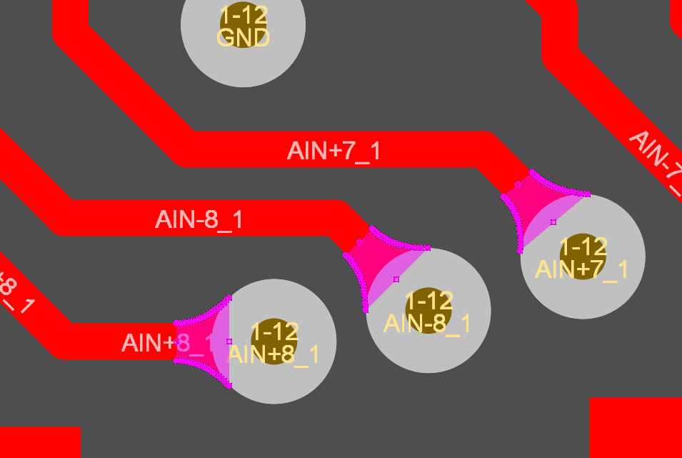
Table of Contents
During the PCB fabrication & manufacturing process, there is always a concern of design quality, high yield, and preventing rework or scrapped boards. If you have even one printed board design under your belt, you have probably already been exposed to a host of unexpected problems at various stages of development. However, there are some simple design decisions that designers can make to prevent low yield and ensure high reliability during operation.
One problem that commonly arises during fabrication is misaligned holes and undesirable breakouts due to drill wander. Even if they don’t cause the board to be rejected, they can lead to problems with track separation over time. Despite them being so common, and seemingly beyond your control, what measures can you take to prepare for and prevent these issues from occurring in your designs? Thankfully, PCB teardrop yielding on your vias and landing pads help ensure a missed drill hit can still form a reliable connection, while also preventing track separation.
PCB Teardrops in Your Layout
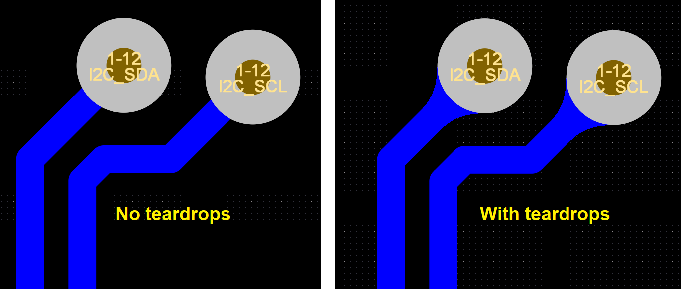
Teardrops are a simple addition to a trace that makes a connection to a landing pad. An example is shown below, where I2C lines are connected to vias in a PCB layout. In the image below, the PCB teardrop is some extra copper that fillets out from the trace to the edge of the via's annular ring. By adding this extra copper, the trace has a stronger connection to the annular ring on the via. The format shown below is probably the most common style of PCB teardrop used on vias. The other teardrop style is sometimes called the snowman style as it adds a small circular section at the trace-to-via connection, rather than using a filleted copper section.
Teardrops on Pads and Traces
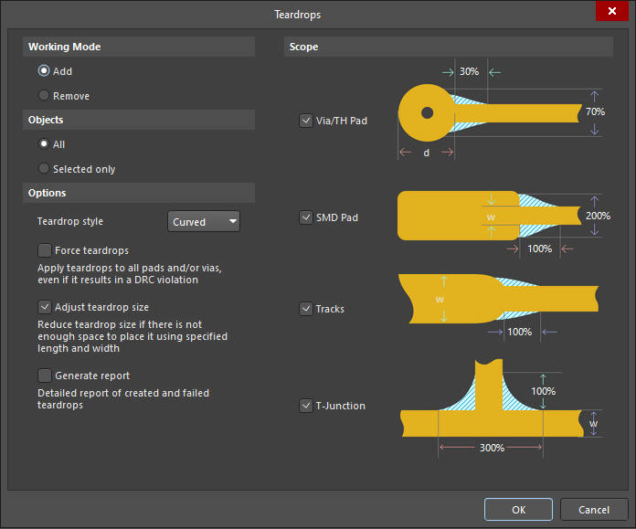
PCB teardrops are not limited to annular rings on via, although this is one of the most common places they can be found in PCBs for high reliability applications. In addition to vias, PCB teardrops can be added to SMD pads, right-angle connections between traces, and locations where a trace transitions from wide to narrow width. These formats are shown below.
Why Use PCB Teardrops?
During the PCB fabrication processes, are two potential problems that can occur when drilling a typical PCB:
- The drill bit may wander during fabrication as there is some very slight inaccuracy and hysteresis in CNC translation stages. As such, the hole and drill can get slightly misaligned, and the drill hole may not line up perfectly with the pad location.
- Layers can shift very slightly during lamination, which results in misalignment of pads on different layers. The drill can hit perfectly on one layer, but it may be misaligned on another layer.
PCB teardrops are your insurance policy against drill wander and layer misalignment during fabrication. If misalignment is severe, there is still a high chance the drill hit will not sever the connection between the pad and via. The extra copper will still provide a connection that can be plated.
The other reason teardrops are used in a PCB layout is to provide extra strength so that the vias can withstand thermal and mechanical stress. By placing a fillet, we don't have stress concentration at the connection between a thin trace and the pad or via ring. Instead, force on the trace-pad interface will be spread over a larger area, which reduces mechanical stress.
Mechanical and thermal stress can arise in a PCB layout during fabrication and during actual operation. In cases with extreme thermal cycling or mechanical shock, a weak interface between a trace and pad can separate or even fracture. This can occur in both rigid and flexible designs. If this happens during fabrication or assembly, a board will have to be scrapped.
PCB Teardrops and IPC Standards
The IPC standards for reliability are divided into Class 1-3. Designs adhering to Class 3 are intended to have highest possible reliability, with applications areas including military electronics and life support equipment. Devices classified as Class 3 need to have minimum possible downtime and longest possible lifetime. Class 3 products also have exacting fabrication and assembly standards that are intended to ensure reliability.
Various IPC standards call out specific and generic requirements for Class 3 products. Among the various design and fabrication standards, IPC 6012 and IPC 2221A specify requirements on annular rings, blind/buried vias, component overhang, solder joints, and much more. Although IPC standards do not place specific design requirements on teardrops, they are mentioned in IPC 2221A as a recommended method to ensure reliability. In Class 3 designs, it's highly recommended to use teardrops on annular rings for all vias.
Including teardrops in your next design is an important step in DFM. You can use printed circuit board teardrops to provide increased reliability more copper supports around drilled holes when you have the right set of layout and routing tools. Teardrops are easy to use in Altium Designer® to establish stronger track-to-pad, track-to-via, and track-to-track connections at the click of a mouse.
Download a free white paper about using teardrops in your next PCB design for improved quality and yield. If you want to learn more about all the features in Altium Designer, talk to an Altium expert today.


