Composite Amplifiers and How They Give the Best of Both Worlds
Table of Contents

There are many times where you need an amplifier with high gain, low noise, high slew rate, and broad bandwidth simultaneously. However, not all of these design goals are possible with all off-the-shelf components. One solution is creative use of multiple amplifiers in a composite amplifier design. With the right composite amplifier, you can create a unique amplifier that exploits the best characteristics of each amplifier stage. Here are some points to consider when working with a composite amplifier design and how to evaluate your design with the right set of circuit simulation tools.
Understanding Composite Amplifiers
Every composite amplifier involves at least two amplifiers. The typical circuit diagram involves two op-amps, but a real composite amplifier could involve more than two amplifiers. This is similar to a cascaded or multistage amplifier, and it helps to distinguish between each type of amplifier to more easily see the potential advantages of a composite amplifier.
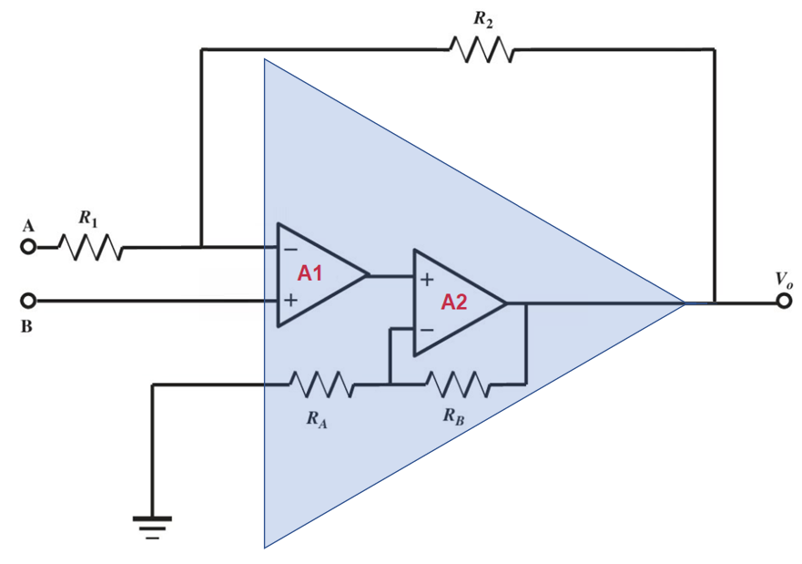
Composite Amplifier Circuit Diagram
The image below shows a general example of a composite amplifier circuit diagram. Each amplifier in this example is an operational amplifier that is implemented in the classical manner that most designers are familiar with. There is shared feedback between the output and the first amplifier A1. The second amplifier A2 has its own feedback loop in addition to the shared feedback for the entire composite amplifier. In this way, the second amplifier is essentially part of the feedback loop in the first amplifier, which is formed with the loop A2 → R2 → A1.
Multistage vs. Cascaded vs. Composite Amplifiers
These different types of amplifiers can be confused with each other, and for good reason. A multistage amplifier will contain an amplifier in each stage, where each stage may have its own topology or involve multiple amplifiers (including a composite amplifier). All cascaded amplifiers are multistage amplifiers, but the converse is not necessarily correct. In fact, the terms "multistage amplifier" and "cascaded amplifier" are sometimes used interchangeably.
The main factor that distinguishes these different types of amplifiers is how the gains (really the transfer functions) from each amplifier will combine to produce the gain (transfer function) of the entire amplifier in the linear regime. For a cascaded amplifier or multistage amplifier, the total gain is just the products of the individual gains from each amplifier, assuming that all amplifier stages are operating in their respective linear regimes. This is not the case for a composite amplifier in general. As we can see from the above circuit diagram, the total gain depends on how shared feedback and the second-stage feedback are implemented. The table below shows a short summary of these different types of amplifiers and how feedback arises between different stages.
|
|
|
|
|
|
|
|
|
|
|
|
|
|
|
|
Composite Amplifier Design
Gain-Bandwidth
There are a few basic points to understand about the construction of a composite amplifier. The first is the relation between the composite gain of the overall composite amplifier (set by R1 and R2 in the above circuit diagram) and the individual gains of each amplifier. Although the gains are multiplicative, the gain of A1 is (Total Gain)/(Gain of A2); it is set entirely by the output from A2 and the shared feedback loop. The goal in setting gain bandwidth is to prevent individual amplifiers from peaking, which will prevent peaking in the composite transfer function. The rolloff will match that of a higher-order amplifier (product of the orders of the individual amplifiers).
Secondary Stage
Choosing a second-stage, higher-power amp that is faster than the first stage will increase the stability of the overall design. As an example, amplifiers similar to the ADA4870 are a good option as they tend to be unaffected by gain-bandwidth product variations. This, in turn, leaves the bandwidth of the second amp independent of the gain and can be adjusted by the feedback resistors’ value. This will be an important variable to adjust in optimizing the stability of the circuit.
Frequency Compensation
A simulation tool will help with designing frequency compensation to ensure the amplifier design will not exhibit instabilities in either stage. The goal is to keep the phase margin within limits when driving a capacitive load. Frequency compensation is normally applied with feedback capacitors to set the phase shift back to the first-stage input. Transient analysis and Bode plot analysis in a SPICE simulation with real component models will tell you if the composite amplifier circuit is stable.
If you’re designing an amplification stage for an analog board and you need to use simulations for amplifier stability analysis, the circuit design and layout tools in Altium Designer® can help you optimize your design to prevent oscillations. You can import simulation models for real components, define in your drill table and fabrication documents, and prepare all other deliverables for manufacturing.
When you’ve finished your design, and you want to share your project, the Altium 365™ platform makes it easy to collaborate with other designers. We have only scratched the surface of what is possible to do with Altium Designer on Altium 365. You can check the product page for a more in-depth feature description or one of the On-Demand Webinars.

About Author
Related Resources


Related Technical Documentation


Take advantage of the world's
most trusted PCB design system.
One interface. One data
model. Endless possibilities.
Effortlessly collaborate with
mechanical designers.
The world's most trusted
PCB design platform
Best in class interactive
routing
View License Options
Thank you, you are now subscribed to updates.