PCB Grounding Techniques for Plated PCB Mounting Holes

Table of Contents
- How to Design PCB Mounting Holes
- PCB Grounding Techniques and Mounting Holes
- Case 1: Low Current DC, No Galvanic Isolation
- Problems With Case 1 in a Metal Enclosure
- Case 2: High Current with Galvanic Isolation
- Basic Tips For Designing PCB Mounting Holes
- Check out Altium Designer in action...
- Powerful PCB Design
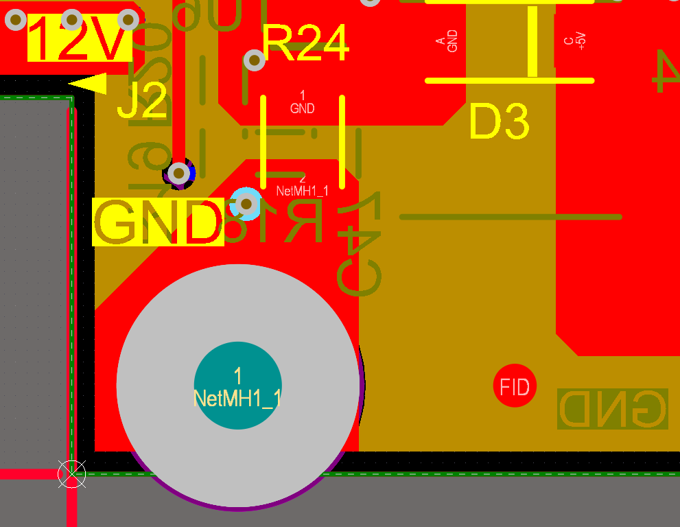
Whenever you place your board into an enclosure, it will need to mount to that enclosure somehow. In order to provide a secure mount without damaging the surface of the PCB with a screw, it's typical to simply place plated through holes in the corners. These PCB mounting holes generally have the pad exposed beneath solder mask so that, if needed, the mounting point can be connected electrically back to one of your nets. One question that often arises in this instance is the grounding and PCB mounting holes. Should mounting be grounded in the design, and if so, how should they be grounded? Should they always be connected to chassis, only to an internal ground, or somewhere else?
This is a fun question, and the answer is typically framed as an "always/never" situation. One person will claim they always ground their mounting holes to an enclosure, while another person will claim it should never be done as it will ruin the design. Like most design rules that are framed this way, the real answer is more complicated and involves many aspects of a design, ranging from input power to the structure of your grounding system. If you understand how power and ground are defined on the input to your PCB, it will be easier to design a mounting strategy that properly accounts for ground.
How to Design PCB Mounting Holes
As the name implies, PCB mounting holes are used to secure your circuit board to an enclosure. There are a few points that everyone agrees on when it comes to PCB mounting holes:
- Mounting holes should generally be plated as this allows mounting with metal screws.
- Because floating bits of metal can be sources of EMI, the mounting holes should be connected to some ground net (earth (PE), signal ground (SGND), a grounded enclosure, etc.).
- Mounting holes should be sized to accommodate some standard-size fastener.
- Mounting holes can be non-plated, although this is only a desirable practice with plastic screws or standoffs used in the design.
I discussed this in a bit of detail in an earlier article on tooling holes, primarily because some prominent resources do not distinguish between mounting holes and tooling holes. For designers, this is an important distinction as mounting holes will almost certainly become part of your board's grounding system, and you should consider exactly how that will affect EMI and safety in your design.
Connecting plated mounting holes to the enclosure is a best practice, and your chassis ground might be connected to an earth ground if such a connection is available. However, this is not always the case, such as in a battery-powered system with metal elements in the enclosure. Depending on how PCB mounting holes, the enclosure, and earth are connected, the device could experience EMI or produce an electric shock for the user. The latter case is one problem that might happen in a computer power when the supply’s chassis is not well-grounded to earth (while plugged in) or to the negative supply terminal (when unplugged). If PCB grounding techniques are implemented properly, including with a proper earth ground connection, then any floating ground connection can be eliminated, which is one of the primary uses of grounded PCB mounting holes in a metal enclosure.
PCB Grounding Techniques and Mounting Holes
The above image should not be taken as an over-generalization; in some cases you may not need the mounting hole to be grounded to the board at all, and instead to be grounded to the enclosure. In other cases, you won't have a choice: you have to ground the mounting hole to an internal connection because there is nowhere else to ground it. The PCB grounding technique you apply to a mounting hole should account for the current you need to handle, the frequency of that current, and safety issues such as ESD. Unfortunately, there is no single approach that addresses every possible situation, but hopefully the points below illustrate how to think about ground connections that arise when mounting a PCB.
Case 1: Low Current DC, No Galvanic Isolation
The tables below show a few situations that should illustrate how to deal with a plated PCB mounting hole as part of standard PCB grounding techniques. Here, we're considering cases with 3-wire DC (POS, NEG, and an earth GND connection), 2-wire DC (POS and NEG only), and 3-wire AC rectified to DC.
|
|
|
|
|
|
|
|
|
|
|
|
|
|
|
|
Obviously, these aren’t the only possible situations where you will have to deal with defining GND at low current. These guidelines are primarily intended for EMI suppression from the metal enclosure (or a plastic enclosure with metal elements) by setting the enclosure and PCB ground to the same potential.
In the 3-wire system, and in the 3-wire AC/2-wire DC system, if you must connect the PE and negative supply GND inside the system, do so at the input point. In this way, you're preventing GND loops and ensuring the metal elements in the enclosure provide shielding and are not floating. This mimics residential wiring: the connection between your circuit ground and system ground is only supplied at the system input (e.g., at the breaker), but NOT at the point where power is returned to GND. However, that connection is typically created at the plug on in your wall outlet/breaker, and making an additional connection from the board to the enclosure may create a small ground loop through the input cable.
Problems With Case 1 in a Metal Enclosure
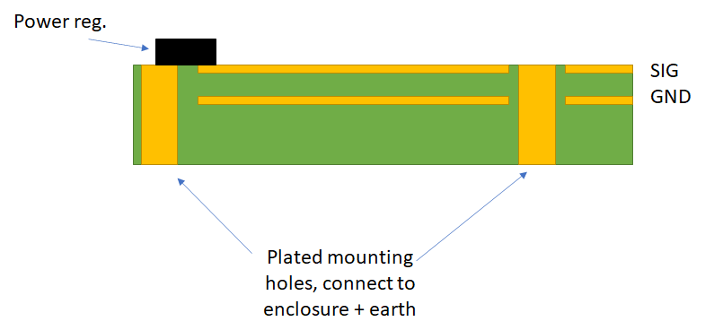
3-wire DC with earth/chassis connected: If PCB mounting holes bridge the PCB GND with the enclosure at one point, you could have a GND loop on the cord when the upstream portion of the cord is connected to earth. If connected at multiple points, you have more safety connections to GND and a nice path to earth for stray currents, ESD, etc., but you risk creating DC ground loops around the board via the enclosure (prevent these with solid, low-impedance connections). Even if there is a single plated PCB mounting hole point, you could still have capacitively coupled currents for high-frequency noise, leading to common-mode noise back to the input. The best balance of safety, EMI suppression, and low noise is to plate the mounting holes, connect them to the metal enclosure, but leave these disconnected from the PCB's signal ground; you can always create paths for ESD with suppression circuits if needed.
There are some potential problems with this. You have to ensure a low impedance connection to earth if you want to have any safety effect
3-wire power rectified to 2-wire: If the enclosure is metalized, then you should only bridge the PCB GND with the enclosure through the plated mounting holes. This would apply when your cable is unshielded and only feeds in through two wires. However, when everything (rectifier + DC output) is on one board, you should follow the previous guidelines for a general 3-wire system. Be careful here with possible GND loops; DC may have loop problems through the enclosure/GND plane if there are multiple mounting hole connections to GND, but multiple connections are generally preferred if your problem is high frequency noise or the possibility of multiple ESD sources at different points on the board. Think about the specific problem you want to solve
2-wire DC: This case occurs when you have a battery or a bench-top power supply and it can be equivalent to the previous case. Again, think about the specific problem you want to solve before going this route; you'll want to ensure your grounding strategy accounts for the problems you need to solve as there is no single grounding method that solves every problem. I mention this here because, in today's electronics, may devices will use exactly this 2-wire configuration and will try to balance safety against RF noise while trying to suppress common-mode noise.
If you're dealing with a battery, the currents are generally low enough that, as long as you have very low impedance connections at the power supply input, you can bridge the enclosure with the board GND through plated PCB mounting holes. Ideally this happens at one point (the power supply input) if you just want to tie grounds together and ensure nothing is floating. Doing this at multiple points offers greater safety against ESD/stray currents in different locations, especially near connectors (see industrial Ethernet as an example); this is basically what your laptop does with its metal case when it is unplugged. However, you now have currents moving through the case (and possibly through the user) and the possibility of ground loops, both being bad for user safety and precision measurement applications.

The ideal situation I'm describing for the 3-wire DC power system and 3-wire/2-wire rectified DC power system is to connect earth and enclosure through a single mounting hole at the power input, and only with the mounting hole grounded to the PCB ground. The impedance between the enclosure and earth should be as low as possible, generally involving a large screw or grounding lug.
Unfortunately, grounding everything with one plated PCB mounting hole at the input is not always practical; PCBs with one mounting hole might have that hole placed in the center of the board, which is not always the power input. Generally, there are multiple mounting holes; these are typically at the corners of the board, but a large board could have these distributed around the PCB to provide structural support and prevent vibration. If all the mounting holes are plated and make the same board-to-enclosure connection, then you have the possibility of ground loops. Then there is always some capacitive coupling for high-frequency noise, creating common-mode noise circulating back to the I/O side of the board, i.e., a capacitively coupled ground loop for high frequency noise.
Clearly, there is a need to balance "use multiple plated mounting holes to provide maximum ESD safety", "use one plated mounting hole and leave all others un-plated to prevent ground loops and noise", and "ensure the case is grounded for low EMI and high shielding". Carefully consider your design requirements before bridging your PCB GND with the enclosure and earth using plated mounting holes.
Case 2: High Current with Galvanic Isolation
This case can be tricky as noise is not always the major problem here, the problem is one of safety. This type of system is common for power supplies, and one goal in providing galvanic isolation is to prevent a shock from the primary side from reaching the output side. Furthermore, we don't want to destroy isolation by bridging the input and output sides of the system with connections to the enclosure. Therefore, use an earth connection on the enclosure, and connect the PCB with plated mounting holes only to the chassis.
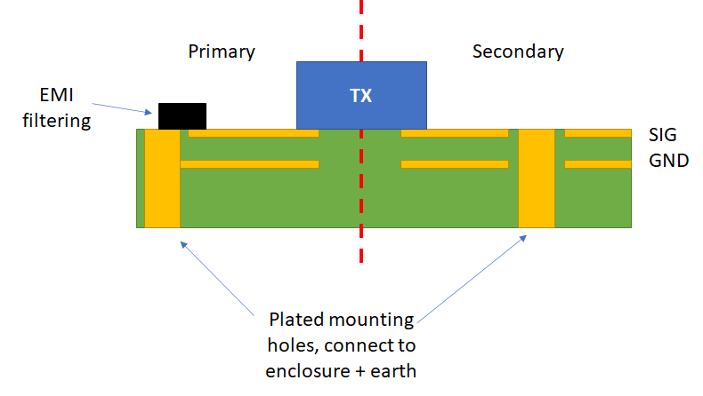
In this case, it's highly recommended to ground the chassis to earth, make a PCB GND-earth connection only at the power input, and then use plated mounting holes to connect only to the chassis. This is shown in the above image. On the secondary/output side of an isolated system, do the same: only connect plated mounting holes to the chassis, but not to the PCB GND on the secondary side. To prevent noisy radiated emission from the secondary GND region, bridge the primary and secondary GND regions with a Class Y capacitor. This will ensure galvanic isolation for DC currents, but it will ensure all GND regions are at the same potential for AC currents.
Basic Tips For Designing PCB Mounting Holes
A PCB mounting hole is really an electrical feature that you may take for granted in your design. From a mechanical standpoint, make sure you size these with a sufficiently large hole and pad to accept a fastener while still allowing a low-impedance electrical connection to the chassis if needed. Aside from these points, it's important to remember that simply grounding out all of your mounting holes to a metal enclosure will not solve every problem. The PCB grounding techniques you implement with your mounting holes don't solve every EMI or safety problem, so be sure to craft a grounding strategy that addresses your specific problems in your system.
When you need the best layout tools for placing PCB mounting holes, look to the complete set of PCB design features in Altium Designer®. As you build your layer stack and define nets in your schematics, you'll be able to implement the PCB grounding techniques your system needs to ensure EMI suppression and safety. When you’ve finished your design, and you want to release files to your manufacturer, the Altium 365™ platform makes it easy to collaborate and share your projects.
We have only scratched the surface of what’s possible with Altium Designer on Altium 365. Start your free trial of Altium Designer + Altium 365 today.
Check out Altium Designer in action...
Powerful PCB Design

About Author
Related Resources


Related Technical Documentation


Take advantage of the world's
most trusted PCB design system.
One interface. One data
model. Endless possibilities.
Effortlessly collaborate with
mechanical designers.
The world's most trusted
PCB design platform
Best in class interactive
routing
View License Options
Thank you, you are now subscribed to updates.