Kick Your EDA Translations to the Curb: Choose Unified Design
Table of Contents
Personal computing devices have significantly changed how bills are paid. And it’s getting better as utilities, banks, and medical enterprises get onboard with unified, intuitive user interfaces. Not long ago, moving from writing and mailing checks to using online banking for paying bills was excruciating. All the environments and web pages were slightly different. Even the simple process of paying a bill was inconsistent and there was no guarantee that the transaction actually occurred once you hit the “send” button.
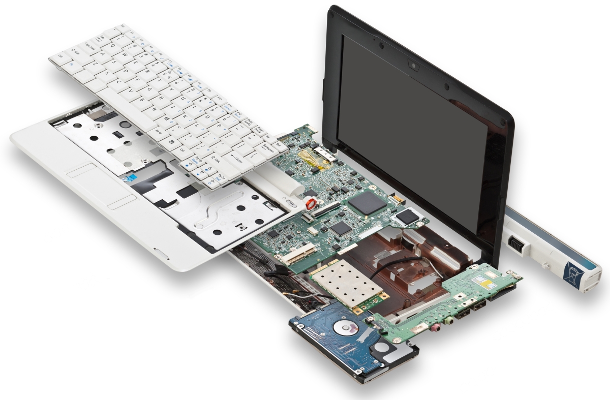
These days, the EDA software landscape is undergoing a similar evolution as early electronic bill paying and banking. Each step in the printed circuit assembly process, from schematic capture and layout to BOM generation, is performed on a different software tool. Each environment is built on a slightly different underlying framework so using them together is a disordered process. It has been apparent for years that these tools share information that should be linked, so the industry has provided translators to facilitate EDA tool instantiation communication. And although the translators helped integrate the most vital associations, they produce disjointed environments with many discontinuities. Too many of the steps are ill-defined or don’t work well with one another. Each environment is custom and interfaces can be significantly different.
Using Translators for EDA Software is Disordered
Given the different frameworks and associated interfaces, it’s no wonder that the tools struggle to play well together. But combining the complex tools by going back and starting over has been impossible for EDA vendors. It takes years to develop these tools. As a result, EDA software tooling environments continue to be an amalgamation of disordered tool instantiations. The instantiations individually provide tools for schematic capture, PCB layout, component libraries and Bills of Material, and output file containers. As each tool within the environment was built as a standalone, it may not incorporate the framework to easily work with partner software tools.
Remove disorganization from your EDA tool environment with unified tools
This lack of synchronization leads to using translators so partner EDA tools can work together. As each instantiation of the tool was developed on a unique platform, it is a complex exercise to provide elegant communication between the tools to transfer design results. The translators port the most important pieces of the design information, but woefully, many details are lost in translation, causing discontinuities as vital information is sacrificed. Although tool vendors react by offering updates to the existing tools, it is difficult to smoothen out discontinuities.
Extra Work Results from Discontinuities Introduced by Translators
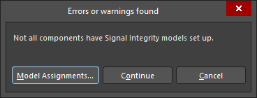
Discontinuities result from unique platforms that don’t translate easily across tools. This leaves users facing large learning curves for each tool. More time is needed, as well, to understand the translator’s abilities so the results are understandable once the translation is made. This becomes obvious when error messages appear on the PC screen containing hundreds of error statements.
These error statements contain bundles of pseudo-errors, each of which needs to be manually checked to ensure a real error isn’t missed. It can take entire afternoons that stretch into another morning just to wade through and check each error. Undeniably, this process is excruciating and time-consuming, which leaves users to wonder: why haven’t vendors figured out how to revise their tools to automate detailed work?
Keep the ideas flowing with intelligent EDA tools
Each error must be checked while navigating two separate EDA software frameworks to intricately map source placement to resultant occurrence across tools. It takes hours to meticulously check each detail of every placed component along with its nets. Netlists that were previously functional break down during translation. Component assignments become skewed and are seen to be off their pads, going from Schematic to PCB layout. Rules are broken and constraints are misinterpreted. It is a never-ending ordeal requiring hours, or sometimes days, of manual analysis to understand and resolve each discontinuity.
Adopting Unified EDA Tools Provides Intelligent Interfaces
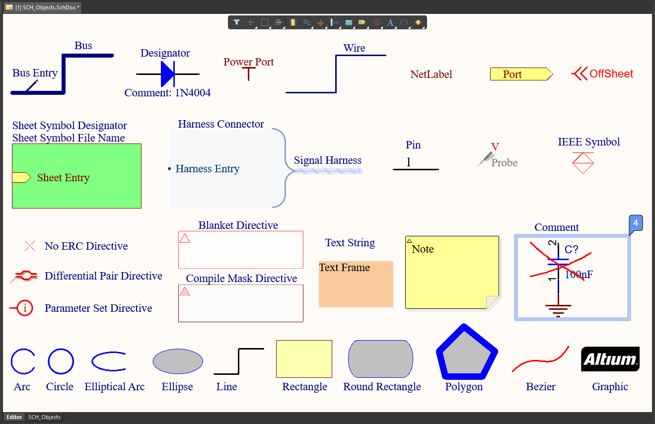
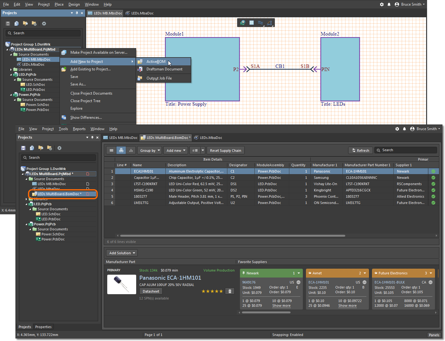
What’s needed is EDA software that is built from the ground up and includes a framework with all the tools needed for printed circuit assembly design and manufacture. This entails a unified framework that includes Schematic capture, PCB layout, Bill of Material, and output file containers all in the same environment. When EDA tools exist within the same framework and environment, built together from the ground up, their editors and menus all look familiar. There is no steep learning curve required when moving from one to the other.
Altium Designer 18 offers a modern unified design environment with a platform that offers logical and physical presentations within the tools. The tools are always integrated at the system level, while the editors and menus within each tool in the unified environment have familiar editors and sub-menus to ease the design process. The tools support designers’ needs without a steep learning curve, which enables designers to focus on critical design-related work.
If you’d like to kick your discontinuous EDA tools to the curb and adopt the unification platform, talk to an Altium expert today.
Start the journey to switch over to Altium Designer today.
“During the first days of working with Altium, like any new tool, I was a bit hesitant to easily accept it but it took very reasonable time (less than two weeks) to learn how to use Altium efficiently and effectively. There are plenty of online learning materials available for Altium Designer. Some neat features that I like very much about Altium are: Grouping signals/nets, classes, differential pairs, DRC, Polygon Management, Layer Stack Management, components 3D body Unlike some other products, choosing the right option/package to fulfill your needs is very straight forward in Altium. Besides Altium has a very competitive pricing. I highly recommend using Altium if you want a professional tool within a reasonable budget.”
- President at Industrial Automation and Medical Equipment Design Company


