Technological Development Made Easy as Pie with Historical Altium Designer
Table of Contents
Some words constantly pop-up in daily conversation. Think about how often the word “easy” is used, whether in a bumper sticker that says, “Easy Does It” or a childhood favorite, Easy Bake Ovens. We tell people to “take it easy” and refer to New Orleans as the “Big Easy.” I’m reasonably certain that a guide or book somewhere out there proclaims the “12 Easy Steps to Becoming a Nuclear Scientist.”
In a 1940s film called “The Long Voyage Home,” a character advised another to handle a suspicious box “easy peasy lemon squeezy,” which translates as “extremely easy”. In the PCB world, “easy” isn’t a term that is used lightly. However, Altium ® has made PCB design considerably easier through an improved interface that offers users the ability to move through the PCB design process across the symbol, footprint, schematic, PCB documentation, and other editors.
Because Altium functions as a unified design environment, you can access the tools needed for hardware simulation, PCB design, data management, and design management. Every component contains schematic symbols, BOM, and other parametric data. All this allows you to respond to the demand for high-speed PCB designs.
As Easy as Pie
During the mid-19th century, Americans began using “pie” to describe something pleasant that can be achieved with ease. While making a pie isn’t exactly “easy” unless you’re an experienced baker, working with schematic capture within Altium is.
No matter the decade you’re looking at, printed circuit boards have been rapidly developing for over a hundred years. If you’re familiar with the process of technological revolution, development and innovation efficiencies do not tend to become maximized until the market has solidified. What’s unique about CAD tools and PCB design software is that these design elements were made before technology had completed branching out and creating various industries.
It is great that PCB design tools were capable of assisting in the innovation process for technological development; however, the difficulty is that design tools become their own industry, forced to develop, maximize efficiency, and innovate alongside the blossoming industries design software attempts to prioritize.
From your first schematic to your full design produced, Altium is there for you.
When considering the history of printed circuit boards, it makes it easier to understand where you want your design software to stand. A software tool that adapts, throughout the centuries. Thankfully, whether you know them as ® or Altium, Altium has and always will be the tool that leads the pack in adapting to industrial innovation and technological development. The unified interface between schematics and the PCB design gives you the capability to add design rules and constraints. Altium also gives PCB design teams unified access to device sheets, snippets, and Smart Paste.
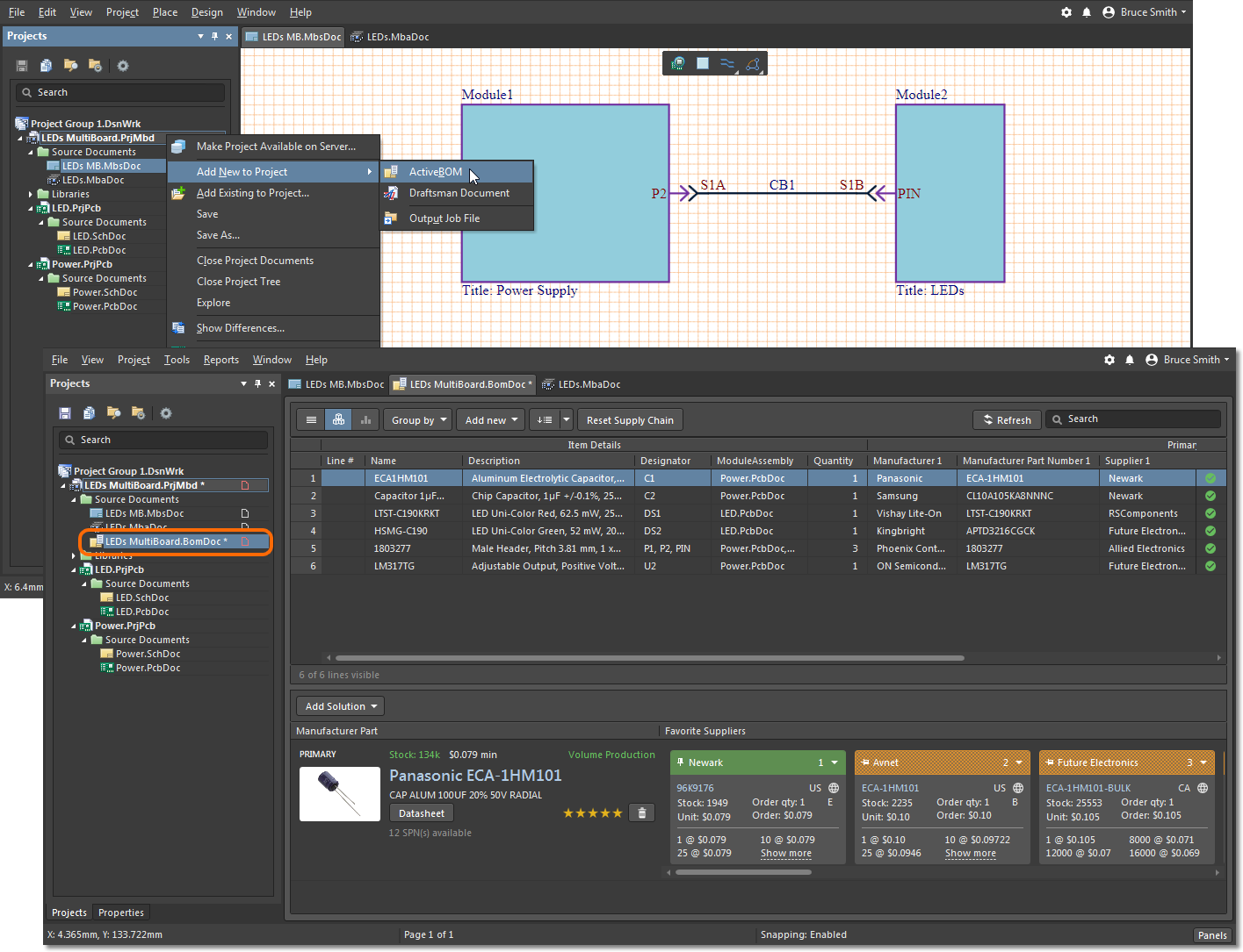
Designed for better productivity, the Properties Panel has the same look and feel no matter whether you’re working in the schematic or PCB editors. While keeping many useful features of older tools, the Properties Panel provides the information and controls for an item selected in the workspace. As a result, you can configure an object before placement. With no item selected, the panel provides unified board options through the document, multi-board document, and active BOM document. This approach allows you to quickly change general document options.
Whoa… Easy Now!
Picture a white-hat-wearing, movie cowboy saying “whoa…easy now!” to calm his trusted horse. Altium’s component management features give you the symbols, footprints, and simulation models that you need to remain calm. You can create components by using the Symbol Wizard and IPC-Compliant Wizard; and if you need to run simulations, you can easily do so by linking components to IBIS and SPICE models. Furthermore, you can gain real-time BOM management by using ® to source all components in your project.
Easy Come, Easy Go
Though “easy come, easy go,” is an ancient Chinese idiom, the meaning has grown to be universally understood. Instead of offering limited short-term solutions for board layout, Altium gives you the capability to define the shape of your PCB and apply design verification to your pre-route setup through unified access. By combining cross-probing and unified datasets, you can select an object on your schematic and your PCB at the same time. Cross-probing cross-references every net, pin, and component on the PCB with the schematic.
As Easy as Taking Candy From a Baby!
“Taking candy from a baby” originally alluded to performing an impossible task during the mid-1800s. American shipping companies designated dangerous cargo as “C.A.N.D” or “Cargo for Accelerated Nautical Delivery.” Although extremely easy, you can rest assured that nothing dangerous occurs when defining and modifying rigid-flex layer stack regions within Altium. You can define the stack regions with bend lines and angles as well as with full 3D folding and component clearance checking.
3D PCB design enables the thoroughness of today requires
Like within the Properties panel, the View Configuration panel provides the ability to edit and control the layers of the PCB. After switching the 3D setting in the General Settings region to ON, you can control the colors, settings, visibility, 3D settings, and masking through the panel. The 3D settings on the View Options tab allow you to configure the 3D views. With this, you can collaborate with any mechanical to model any complex assembly.
We’re on Easy Street!
Interactive routing takes you to the easy street by allowing you to avoid problems or worries associated with routing. Within Altium, you can use the ® wizard to tune high-speed technologies involving complex signal-path groupings. automatically identifies interfaces and creates rules to keep all signals in sync and tuned to the correct length. Because groups your signals together, you gain organization and improved capabilities for tracing, precise length tuning, and error correction.
® gives you advanced capabilities for user-guided routing automation. The interactive routing tool allows you to select the amount of automation to deploy along selected nets. simultaneously works on multiple layers while complying with your design constraints. Each process yields evenly distributed traces and precise routing. Overall, has many capabilities, which include allowing you to interactively route at any angle, use intelligent push and shove, and quickly route across layers.
The phrase “As Easy as One-Two-Three” speaks to the intuitive qualities of Altium and the level of support provided by Altium. You can find answers to your questions through TECHDOCS, a video, and user forums. Altium’s Support Center also provides solutions for any problem that you may encounter.
To learn more about using Altium to simplify your PCB design process, talk to an expert at Altium.


