Don't Let Lithography Issues Cast a Shadow on Your PCB Manufacturing
Projectors can often be the most annoying piece of technology to work with. You could have a movie night you want to host with an old school projector and some nice, buttery popcorn but be unable to find a spot where the image projected isn’t crooked; you could be trying to give a highly-influential presentation to your peers and bosses, only to encounter that the projector has squished all of your images and graphs; you could be trying to teach a lesson and find that the projector only transmits images in black-and-white. All of the hours you spent getting things to fit on the slide seem wasted because the projected image looks ridiculous. Being able to control the alignment of the projector and its display could resolve so many of these high-stress situations.
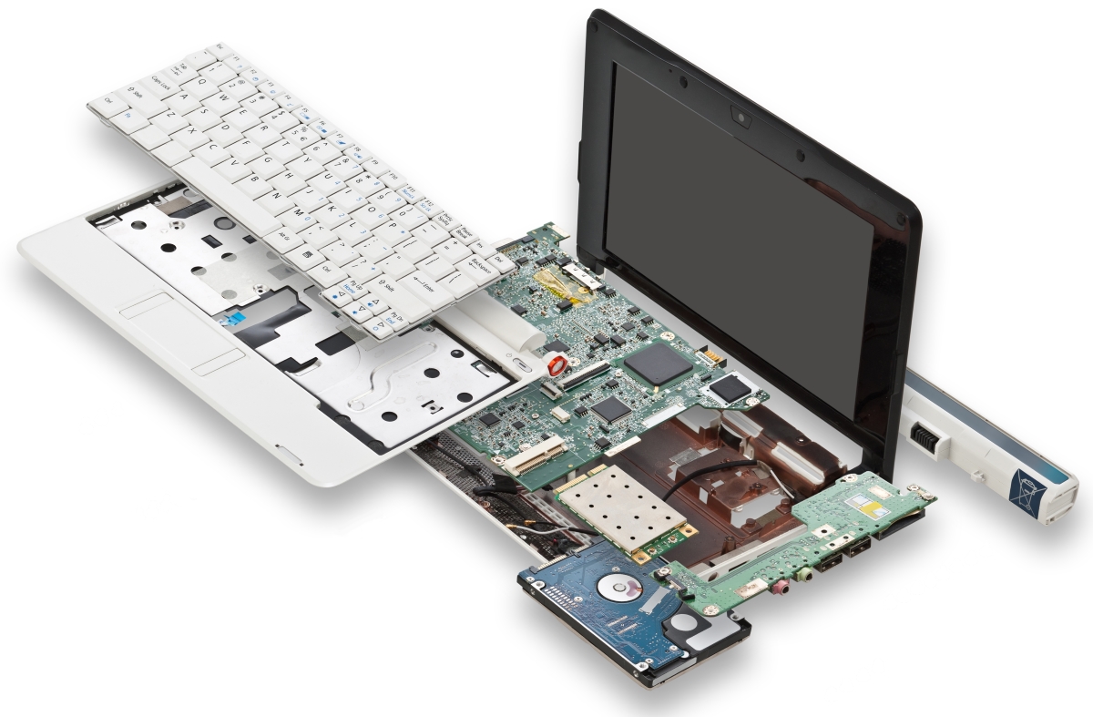
When your PCBs are being manufactured, there are similar optical alignments that take place. They are part of the lithography process to lay down patterned layers as the PCB is built up. Don’t suffer through presenting a crooked slide, and certainly don’t suffer from misaligning your components within a PCB design. Learn how to properly plan out your lithography process, as well as understand the factors which might affect it and cause defects.
How is PCB Manufacturing Affected By Lithography?
The etching and electroplating processes used in PCB manufacturing aren’t very directional. Without a patterned protective coating on the board, everything would be etched, plated, or coated indiscriminately. The protective pattern may be a metal stencil, a sheet of polyamide, or a resist. The manufacturing process dictates which material is most appropriate—you don’t want to use a metal stencil during etching, for example, since the stencil would be damaged and unusable after a few boards.
Resists are light sensitive (called photosensitive in the “biz”) to specific wavelengths of light, usually ultraviolet. A photolithography process is used to expose specific areas to light, so the resist in those areas is cured or hardened. The rest is washed away, leaving specific areas clear for the next stage of processing. The mask (like a stencil for light) used to control which areas are patterned, needs to be aligned with the light source and the PCB to ensure that you don’t get weird effects like the projector screen. Otherwise, you’ll start seeing some defects in the lithography.
Sources of Lithographic Defects
You might not ever get the alignment right on the projector—some things are out of your control. You can keep track of the potential sources for lithographic defects and plan against them, though. Here are some to keep in mind:
Shadows: If your manufacturer keeps the environment clean, hopefully, you’ll never have to deal with this one. Sometimes, though, you’ll get particles falling on the mask and casting shadows when the light should be curing the resist, like putting a chair in front of a projector and cutting off a small part of the image. That means some areas won’t harden the way they’re supposed to and instead will get etched during the next processing steps.
Dose and exposure issues: The “dose” of light that a resist gets exposed to is calculated like an integral—it’s the brightness of the light over the total exposure time. If the timing is off, or the light is too dim, the resist might not get a high enough dose to harden all the way. Sometimes, the light source isn’t uniform, so the curing is correspondingly uneven across the resist. The results here vary. You might be fine if the etching or plating step is quick and your manufacturer has a tough resist. Or, you might see resist start flaking off during the next step and a little bit of the board starts to get exposed to something it shouldn’t.
Aspect ratios: A issue is a slight angular misalignment of either the light, the mask, or the PCB. It’s the same as a projector at the wrong angle, making the top and the bottom of your slides different widths. On your PCB, that means the resist mask will be applied with an incorrect aspect ratio (the aperture width vs the stencil thickness). When the board is done, you’ll have a higher risk of poor quality solder joints, which frequently result in open circuits. If the board isn’t cured properly, you may also have inner and outer layers experiencing shrinkage, expansion and warping at different rates, which can cause aspect ratio issues, too. That’s not only true of photolithography and can cause warpage in your board later on. This kind of shrinking and expansion is often due to CTE mismatch which is also affected by overall PCB size, with large boards being more prone to issues.
Alignment: Misalignment can also be a horizontal or vertical translation, where patterns are laid down millimeters or less away from where they should have been. As feature sizes decrease, small misalignments have larger impacts, since it’s easier to miss a solder pad or via entirely. With decreasing tolerances, make sure your manufacturer can produce and align with features small enough to match your board specifications.
Tolerance: Tolerance is so crucial, it deserves some additional note. The tolerance around feature size depends on your process. Some etchants are prone to over-etching into regions you need protected, so you need to design your mask layer to account for that. Stenciling a paint or silkscreen layer is much more forgiving.
Just like a whole number of things can go wrong with your presentation—so too can there be other factors that influence your PCB manufacturing process. Your feature size and position also will affect the tolerance; tiny pads very close together don’t have much buffer for mistakes. Some etches are directional and will require a thicker resist layer or better tolerance in the x or y direction. The key here is to work closely with the manufacturer and ensure that you understand the limitations and requirements of the processes that will be used to produce your PCBs. Planning your design around manufacturing capabilities will save you a lot of frustration later.
The masks that are used in lithography are usually generated from the Gerber files in your PCB design. Users can implement DFM practices in their PCB design techniques with the world-class PCB design and layout features in Altium Designer®. Users can take advantage of a single integrated design platform with circuit design and PCB layout features for creating manufacturable circuit boards. When you’ve finished your design, and you want to release files to your manufacturer, the Altium 365™ platform makes it easy to collaborate and share your projects.
We have only scratched the surface of what’s possible with Altium Designer on Altium 365. Start your free trial of Altium Designer + Altium 365 today.


