High Speed PCB Design Guidelines: An Overview for Getting Started

Table of Contents
One of the most common questions I receive from new designers and new hardware developers relates to the differences between high-speed digital designs and any other circuit board. Everyone naturally assumes the clock frequency defines the limit where we consider a design to be operating at high speed, but this is not the whole story. High speed designs can be identified by the presence of two common characteristics:
- The presence of standardized digital computing interfaces like USB, DDR, PCIe, Ethernet, or vision interfaces like CSI-2
- The need for prescribed impedance in signaling standards in order to successfully deliver data to its destination
High-speed digital PCB designs can experience many of the same problems as high-frequency PCBs, which is why many high-speed PCB design guidelines incorporate some elements of RF design. Getting to a successful high-speed design takes a clear layout strategy that helps you arrange components and route easily, as well as obey some basic design rules that can help you stay successful. Before you start floorplanning your next high-speed design and start placement, keep these points in mind as these will help ensure success.
Main Factors That Drive High Speed PCB Design
If you're unfamiliar with the core concepts in high-speed PCB design, read this tutorial before getting started.
Modern digital systems do not use small logic circuits; this is something you might have seen decades ago. Today, digital systems are typically designed around some central processor that provides all the core data collection and processing functions that need to be performed during operations. The main processor will run the core application that orchestrates data transmission between components in the PCB. It's common to build a high-speed PCB layout entirely around a single processor with some ASIC peripherals that implement the required functions. Placement of these main components will drive how you route the board and design your stackup to support your routing strategy.
Placement of Large ICs
Host processors in a high-speed PCB could be a microcontroller or a large, specialized processor like an FPGA. These components might have very high pin counts that connect to power, ground, I/Os, and even analog interfaces. No matter what type of chip is being used as the host processor in the device, it is the capabilities of this device that will drive the need for creative routing and floorplanning in the PCB layout. In many high speed digital systems, we can draw out the kind of floorplan shown below.
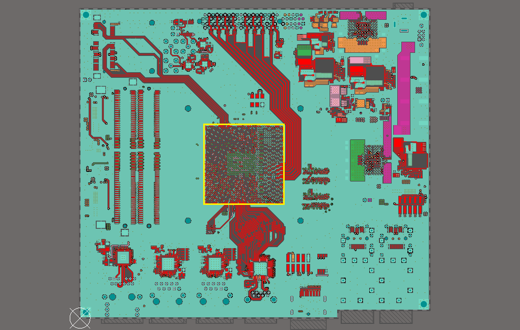
This component placement is based on some simple guidelines:
- Centrally locate it so that all the interfaces are accessible.
- Orient it so that peripherals can be placed close to their interfaces.
This should explain why so many high-speed digital systems, like computer motherboards, have a relatively centrally-located CPU; they are ensuring all the peripherals can access it when routing. After placement is completed and finalized, you can consider how to route the PCB so that impedance targets are hit and so that interfaces do not interfere with each other.
PCB Stackups for High Speed PCB Routing
Aside from placement, everything else that happens in a high speed PCB is related to the PCB stackup. The stackup must be designed to facilitate routing into components with controlled impedance and while keeping high speed signals relatively separate from each other. We'll look at the component selection aspect first as this can place some constraints on the layer stack, such as the number and thickness of required layers and the amount of power and ground needed. How your board stackup is structured will make a difference in your high speed design in terms of signal integrity, power integrity, and EMI/EMC.
The first goal in stackup design is to determine the number of signal layers you'll need to support high speed routing for all your interfaces. At minimum, you'll want an additional two layers for a power-ground plane pair, and you'll need more ground to place between signal layers in the PCB stackup. For very high speed, such as 10G protocols and faster, you might consider a low-loss PTFE material if your routes will be long.

With sufficient ground in place and enough layers to support each interface and set of signals, you can proceed to designing traces to support high speed PCB routing.
Routing High Speed Signals
It's also important to understand how impedance-controlled traces are constructed to hit a target impedance. The stackup and its materials will determine the trace geometry needed to hit a target impedance. Since impedance-controlled high speed interfaces are differential and prone to crosstalk, it's also important to consider the spacing between traces in a differential pair and between nearby routes. Use some calculator tools to get started designing traces to estimate trace dimensions you'll need, then use your PCB impedance calculator in your stackup editor to hit a more precise impedance value.

Once you've determined your trace geometry needed to hit your impedance target, you can set design rules and begin routing. Geometry and length tolerance rules will be used by your routing tools to set the size and span of length tuning sections, as well as enforce the length width you calculated for a target impedance value. Ensuring you route with minimal crosstalk and minimal via transitions takes its own set of strategies; if you considered these points during floorplanning, you are much more likely to be successful. You can learn more in the linked article below.
What Else Matters in High Speed PCB Design?
For beginners in high speed PCB design, the points above will set you up for success when it's time to start routing your board. These points help ensure signal integrity, as well as solvability without excessively large layer count. There are other things to consider in your high speed PCB so that your board can be successfully routed and manufactured:
- Power Integrity: When you start using larger processors that have higher I/O count and higher power requirements, you need to design the PDN such that it can provide stable power at the required switching speed. These larger chips may have multiple rails that need to be isolated from each other, and rail in the PDN will need to have low impedance to ensure stable power delivery. Learn more about power integrity in high speed design.
- Testing and Measurements: During fabrication, assembly, and debugging, certain points on the PCBA will be probed to ensure continuity and data transfer around the PCB. While a manufacturer won't be doing full signal integrity analysis on the fab or assembly line, having access to test points on the board allows you to do this when testing and debugging the PCBA. Learn more about defining and placing test points.
- Mixed-signal design: Most digital systems are not operating with only high speed interfaces, they also use low-speed, RF, and even low-frequency analog components. Try to arrange these so that return paths do not interfere with each other and learn how to predict return paths in the PCB. Learn more about return paths in high speed PCB layout.
When you're ready to work through your toughest layout challenges, follow these high speed PCB design guidelines and use the best design features to build your board with the complete set of design features in Altium Designer®. When you’ve finished your design, and you want to release files to your manufacturer, the Altium 365™ platform makes it easy to collaborate and share your projects.
We have only scratched the surface of what’s possible with Altium Designer on Altium 365. Start your free trial of Altium Designer + Altium 365 today.

About Author
Related Resources


Related Technical Documentation


Take advantage of the world's
most trusted PCB design system.
One interface. One data
model. Endless possibilities.
Effortlessly collaborate with
mechanical designers.
The world's most trusted
PCB design platform
Best in class interactive
routing
View License Options
Thank you, you are now subscribed to updates.