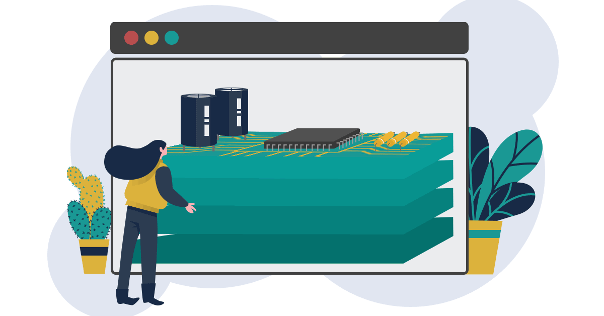
How to Make a Ground Plane for Your PCB Design

Table of Contents
It used to be that printed circuit boards seemed to have the same basic layer configuration, or at least that’s the way I tend to remember it. This meant that they were usually six-layer multi-layer boards, with a ground plane and a VCC plane. The old CAD systems didn’t really have the ability to do much with Altium power planes except to designate layers as a bottom layer or the like. The most you would see in them would be some “X’s” where there was supposed to be a connection for a thru-hole pin or via that connected to that plane.
Thankfully this all changed long ago. Now instead of being driven by the limitations of those older CAD systems, you can drive the design tools to create the plane layers the way you want them to be. You have the choice of creating a ground plane that is either a positive copper fill or a negative plane depending on what your needs are. Any CAD system can do this, but some are better at it than others. Take Altium Designer for example. This PCB design system does a great job of enabling you to create the planes that you need. Let me show you how to make a ground plane in Altium Designer.
Make Sure that Your Schematic Nets are Correct
Before you create your ground planes or voltage planes in layout, you will want to make sure that your schematic is set up correctly. This means that you have assigned the right net names so that all of your power planes and reference planes can be created correctly in layout. In Altium Designer’s schematic editor, you can either assign a net name to a net, as pictured below, or attach a power port to the net as you see on the right side.

Naming Schematic Nets in Altium Designer
The advantage of the power port is that it will connect across all sheets of your schematic without having to attach an off-sheet connector to a named net. Once your nets are correctly named, you are ready to synchronize your schematic and layout to begin working with your Altium ground planes and power planes.
Using an Internal Plane when Creating a Ground Plane
In Altium Designer, you can create your planes either as a negative (Internal) plane or as a positive plane (Polygon Pour). First, we will look at the process of creating a negative or “Internal” plane within our Altium plane layers.
The first thing to do when creating an internal plane is to add a design layer specifically for the plane. In the picture below, you can see that two layers have been added as internal planes in the layer stack manager, which is found in the “Design” pulldown menu. They have been named “GND” and “PWR” respectively and occupy layers two and three. These two internal plane layers also have a “Pullback” value assigned to them which will keep their edges 20 mils away from the edge of the board.
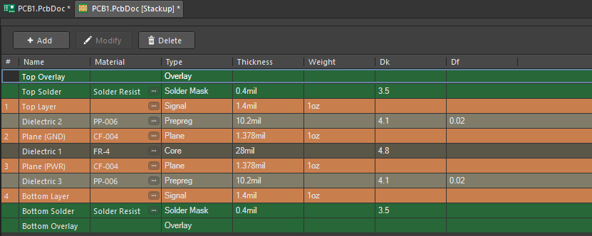
Creating Internal Plane layers using Altium Designer’s Layer Stack Manager
The next thing to do is to assign the correct size for the thermal relief pads and clearances that you want on your plane layers. To do this we will open up the design rules in Altium Designer which are also found in the “Design” pulldown menu. As you can see in the picture below, you have the ability to specify the expansion, air gap, and conductor width of a thermal relief pad. You can also specify the type of connection you want. In the example below you can see how the pad connection is set for thermal relief while the via connection is set as a direct (solid) connection to the plane.
Setting up thermal relief pads in the design rules of Altium Designer
The menu above also gives you the ability to set other values for your planes. Note on the left side of the picture that in addition to the plane connection style, there are also categories for plane clearances and polygon connect styles.
Once you have set everything up, you are ready to assign the net name to the internal plane layer. On the left side of the picture below, note that the pins and vias do not have any visible connections yet to the Altium power plane. This is because the net name has not been assigned. You can also see on the left side of the connection menu that pops up when you double-click on that layer within the layout session. This same menu is used to name both single and split planes.
Assigning the net name to the internal plane layer
In the drop-down menu on the left side of the picture above we have selected “GND” as the net name that we want for this internal plane. This way it will match the GND net of the pins that you can see in the picture. Once we have made this assignment, the vias are directly connected to the plane and the pins have thermal pad connections as you can see on the right side of the picture. Remember that this is a negative plane, so the metal of the thermal spokes and the plane area is represented by the darker color.
Keep in mind that if your printed circuit board has an antenna, the antenna ground plane can be a critical aspect of the antenna functionality and is worth learning more about.
Using a Polygon Pour when Creating a Ground Plane
Now we’ll create a positive plane or a “Polygon Pour”. On the left side of the picture below you can see that this signal layer does not have any metal on it yet. To create the polygon pour you can either use the pulldown menu command “Place > Polygon Pour”, or you can click on the polygon icon in the active bar at the top of the session window.
Creating a Polygon Pour in Altium Designer
While in the polygon pour mode, you will click where you want to place a vertex of the plane that you are creating. If you make a mistake simply use your backspace key to remove the last placed vertex. Once you are finished, right-click in the workspace to exit the polygon pour mode. On the right side of the picture above, you will see the plane that you created assumes the color of the layer that you are working on. You will note though that there aren’t any connections yet to the pins and vias in this Altium plane layer.
Next, select the plane that you just created and go to the properties panel. As you can see in the picture below, you will have a list of Altium assign net to plane. As you can see, we have selected the GND net.
Assigning the net name to the polygon pour
In addition to selecting the net, there are other options and values that you can set up in this panel for your plane. As you can see above, there are options for copper islands, arcs, and nets as well as setting your plane up as a solid pour or hatched.
While the plane is still selected you will next need to re-pour the plane in order to make a connection to the net name that you just assigned to it. To do this, right-click on the selected plane in the main session window.
Re-pouring the polygon pour to connect the net
In the picture above our right mouse click opened up the “Polygon Actions” menu on our selected plane. To connect the plane to the net we will select “Repour Selected”.
At this point, the net name is associated with the polygon pour that you created. In the picture below you can see that the metal shown in red is now connected directly to the vias and with thermal relief spokes to the pins. This Altium ground plane in your PCB layout is now complete.
A completed polygon pour ground plane in Altium Designer
There is much more in Altium Designer for the creation of power planes and ground connection capabilities than what we have shown you here. Altium Designer is both powerful and flexible, making it one of the best PCB design software systems available. It will provide you with the tools that you need to expertly handle the design challenges that you are working with today.
Would you like to find out more about how to make a ground plane on your next PCB design in Altium Designer? Talk to an expert at Altium Designer.
Related Resources


Related Technical Documentation


Take advantage of the world's
most trusted PCB design system.
One interface. One data
model. Endless possibilities.
Effortlessly collaborate with
mechanical designers.
The world's most trusted
PCB design platform
Best in class interactive
routing
View License Options
Thank you, you are now subscribed to updates.