How to Change Board Sizes in Altium Designer
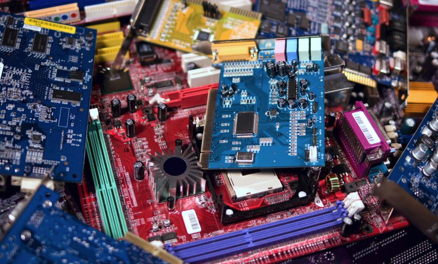
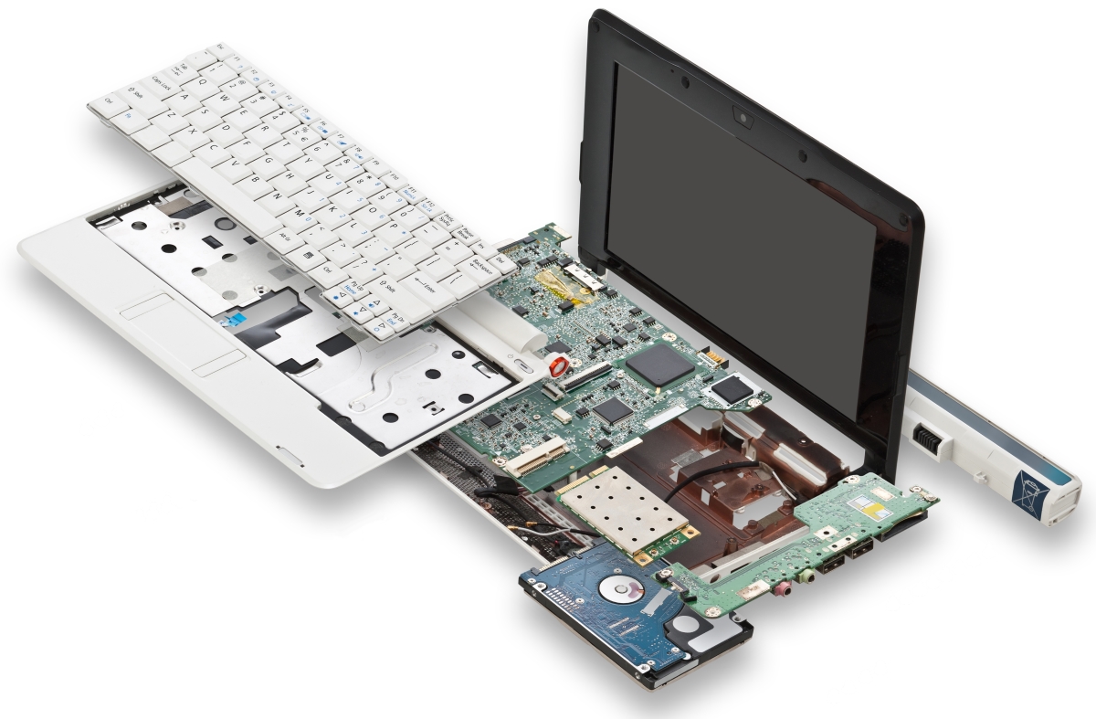
It seems like there are as many different circuit board shapes and sizes as there are stars in the sky. If you have been working for a company that only makes boards according to a few standard form factors, then you may not know just how diverse all of the different sizes and shapes can be. Round boards, square boards, boards with notches and cutouts in them, boards with odd angle corners, and boards with multiple corners and contours.
A list of all the possible different shapes and sizes for PCBs would be endless, but you should know fundamental design rule applications to be ready for any of them.
Fortunately, PCB design tools usually are set up with the drawing utilities that you need to create any board outline that you will come across. The design tools from Altium Designer are particularly well suited for this task and have a lot of options and features to help you. Here we will take a look at a basic layout guide for creating and changing PCB board sizes in Altium Designer®.
Getting Started on Changing Board Sizes in Altium Designer
The first thing that you will want to do is to figure out what PCB size and shape your board needs to be. We won’t spend time on that process as that is usually dictated by the needs of the design or your company.
In more flexible circumstances, many of the PCB design technologies will directly affect the optimal board shape. You can find some very useful information on that by looking at this concise document from Altium Designer on the makeup of printed circuit boards.
Next, you need to have a blank PCB ready to work with in your Altium Designer layout. To do that, you will go to File > New > PCB as you can see in the picture below. You will be prompted for a name and for the purpose of this article we gave our PCB the name of “Test”. With the PCB created in your project, you are now ready to start working on your board outline.
Creating a new PCB in Altium Designer
Creating a Simple Board Outline
Altium Designer opens with a default PCB size of 6-inches by 4-inches in a rectangular board outline (when you create a new PCB object). Often times you can use that board outline and modify it according to your needs as we will do here. The first step will be to set the origin by going to Edit > Origin > Set as you can see on the left side of the picture below.
Setting the origin in your new PCB
Now click your mouse button to set the origin. On the right side of the picture above, you can see that we’ve set up our origin in the bottom left corner of the board outline.
Next, you will want to set your grid. You can do this by using the using the shortcut key of CNTR > Shift > G, or by going to the grid manager in the properties menu of the board. In addition to setting the value and units of your grid, you will also find many other useful functions in the grid manager.
To work with your board outline you must first put Altium Designer into the Board Planning Mode. Altium Designer has three modes for working with the design:
- Board Planning Mode
- 2D Layout Mode
- 3D Layout Mode
You can enter the board planning mode by using the menu selection as shown in the picture below, or by clicking in the board and pressing “1”. In our Test design, entering the board planning mode turns the board outline to a green color which you can also see below.
Setting the board planning mode in Altium Designer
Now you are ready to change PCB board size of the existing board outline in your design session. To do this, you will use the Design > Edit Board Shape pulldown menu command. Once you are in this command you will see the editing handles around the board outline. You can change the size and shape of the board outline by grabbing one of those handles and dragging it to a new location, or by grabbing an edge of the board and dragging it.
Moving a corner while editing the board outline
You can see in the picture above that we have grabbed the upper left editing handle of the Test board outline and pulled it down and to the right. Once we click there, that will become the new location for that corner of the board outline. When you are finished moving the board corners and edges to their desired locations, click outside the board outline to exit the edit mode.
Changing Board Sizes in Altium Designer and Other Features
So far, we’ve shown you how to edit the existing default board outline in an Altium Designer Printed Circuit Board, but there is so much more possible. In the previous section, we used the Design pulldown menu to access the Edit Board Shape command. There are also other board editing commands in this menu, as you can see in the picture below. To use them, remember that you must be in the (green) Board Planning Mode.
The Design pulldown menu in Altium Designer
The design menu gives you a number of options for working on your board outline. You can redefine, edit, modify, and move it. First, let’s look at redefining the board outline.
If the existing board outline is not going to be useful at all to you, you can use the redefine command to create a new board outline from scratch. It will allow you to draw a new board outline by clicking your mouse to place the vertices of the board outline as you can see in the top of the picture below. On the bottom half of the picture, you can see the results of when we completed the new board outline.
Using the Redefine feature to create a new board outline
Another useful function is changing your existing board outline with the modify command. In the left picture below, the modify command allows us to specify a notch in the board outline. On the right side is the finished modification of the board outline with the notch.
Using the Modify feature to create a notch in the board outline
In addition to changing the board outline either by editing, redefining, or modifying it, you can also add cutouts. To do this, you must exit the board planning mode go into the regular 2D-layout mode by using the View menu pulldown or by hitting the “2” key. Once you are there, go into the Design pulldown menu and select Board Shape > Define Board Cutout. Then you will click down the vertices of the cutout as you can see on the top of the picture below, and then right-click the mouse to finish the cutout as you can see on the bottom.
Adding a board cutout in Altium Designer
Altium Designer provides you with five corner modes while creating the shapes for board outlines and cutouts. They are:
- 45 Degree
- 45 Degree with Arc
- 90 Degree
- 90 Degree with Arc
- Any Angle
You can use the Shift > Spacebar to cycle through the five corner modes, and you can also use the spacebar by itself to toggle the direction of the corners. The size of the arc is given to you in text at the bottom of the design session window, and you can increase or decrease the size of the arc by holding down the “.” or “,” keys. To increase the speed of increasing or decreasing the arcs, hold the shift key down while using the “.” and “,” keys.
Working with the arcs takes some dexterity, but practice helps. Don’t forget, if you’ve put in a bad segment while drawing any of this, use the backspace key to remove the last vertex.
The Next Step After Changing Board Sizes in Altium Designer
There are still going to be some things that you will have to do before you can start placing. You will need to transfer the schematic data to the board, configure the board stackup and the visibility of the layers, and set-up your design rules. Once you've got those done though, you will be ready to get into the heart of your PCB layout.
There may be a million different shapes and sizes of circuit boards out there, but fortunately Altium Designer provides you with a great set of PCB design tools to create them with. If you aren’t already using Altium Designer and you would like to find out more, talk to an expert at Altium Designer today.


