Switching Units From MM to Mils and Other PCB Design Measurement Preferences

Table of Contents
Your PCB layout needs to be an accurate reflection of your final design and should follow a specified unit scale. Inside Altium Designer, there are simple ways to set units as you work on the PCB layout, as well as in the schematic where circuits are being created. The short guide below shows how to switch from mm to mil in the Schematic Editor and in the PCB Editor. Users can do this live (while working on the PCB layout) or from the Preferences dialog in both the schematics and PCB.
Fastest Way to Switch Units During Design
Altium Designer offers two unit systems: mm and mil. These are the standard units used in most component datasheets and mechanical drawings, as well as in Gerber files used for PCB fabrication. For anyone who wants to switch units while working in the design, the fastest way to do this depends on if you are in the PCB Editor or the Schematic editor.
- In the Schematic Editor - Change units with the View --> Toggle Units menu option
- In the PCB Editor - There are three options:
- Press "Q" on the keyboard
- Press "V" followed by "U" on the keyboard
- Use the View --> Toggle Units menu option
In addition to the two hotkey options in the PCB editor, Altium Designer helps automate a huge number of tasks with many other hotkeys. You can see some of my favorite hotkeys in this article.
Aside from these options, users can use the Preferences dialog to set or toggle units in the Schematic Editor, or using the Properties panel in the PCB Editor.

Switching Units in the Preferences
Switching from MM to Mils in the Schematic
When you first open up Altium Designer, before you even move to the snap grid, you can set up some preferences for working in the schematic. These preferences can be found by clicking on the gear wheel in the upper right corner of the Altium Designer as shown below. You can also access these preferences with a schematic sheet open by going to the “Tools” pulldown menu and selecting “Preferences.”

Opening the Preferences dialog in Altium Designer
The preferences dialog box gives you the ability to set up how you want the different tools in Altium Designer to behave when you first open them. In the schematic, you can set up behaviors for just about everything from sheet templates to how it is going to zoom into PCB library components. There are also different settings for PCB measurement units as you can see below.
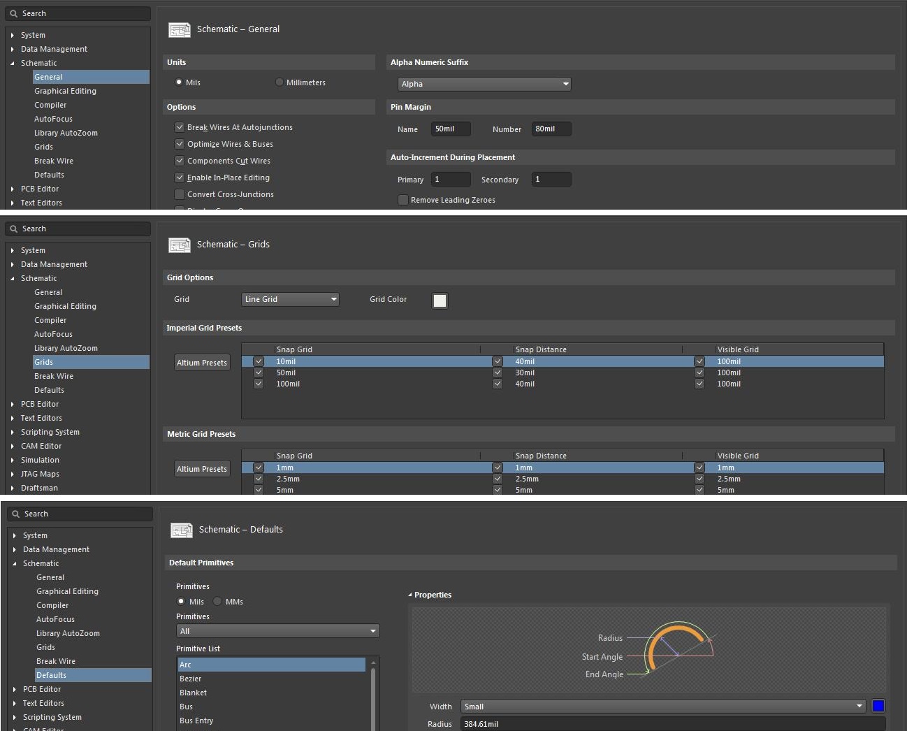
Three different areas where you can set the units in Altium Design’s schematic preferences
In the picture above, you can see three different areas where you can set unit preferences for a new schematic in Altium Designer. The first is the main units for the schematic, which is found in the “General” settings of the preference dialog. The second allows you to set unit preferences for grids, while the third is for setting the units of your default primitive objects.
You are not restricted to the PCB measurement units that were set up in the preferences when working in a schematic, however. You can easily change units on the fly as you work by using the “Toggle Units” command in the “View” pulldown menu. Look closely at the picture below, and you can see that command in the pulldown menu. Notice that the “U” in “Units” is underlined. This means that you can use this letter in a keystroke combination to toggle the units as well. In this case, the command is in the “View” pulldown, so you would need to use the keystroke combination of “vu” to change the units.

The Toggle Units command in the View pulldown menu
Switching from MM to Mils in the PCB Layout
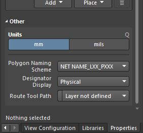
On the PCB layout side of Altium Designer, things a little different. In previous versions of the PCB editor in Altium Designer, the units were changed in the “Board Options” menu. This has now moved to the properties panel, which can be accessed from the “Panels” button. Another thing that we should mention is that instead of “Metric” and “Imperial,” Altium Designer now refers to units of measurement as “MM” (Millimeters) or “Mils” units.
If you’re looking to change your PCB editor measurements, if you need to demonstrate components or traces as imperial units, then you’ll need to locate your board options. To change the units of measurement for the board, open up the “Properties” panel, and scroll down to the bottom. There you can find the units in the “Other” section of the Properties panel, as shown in the picture below.
The units switch in the Properties panel of Altium Designer’s layout tool
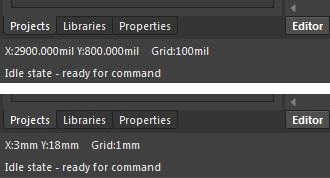
When you change the units, the location and grid data displayed in the lower-left corner of the session window will update. Take a look at the picture below, and you can see the difference in data when we toggle from one unit of measurement to the other. This display of data is also found in the same location in the schematic editor as well.
The display of PCB measurement units in use in Altium Designer
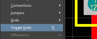
There are some other ways to change the units of measurement in Altium Designer’s layout tool. You can use the command: “Toggle Units” found in the View pulldown menu as shown below. As with the schematic, you can also use the keystroke shortcut combination of “V" followed by "U” on the keyboard to change the units. You also have one other option in layout to change the units, and that is to use "Q" on the keyboard.
The View > Toggle Units command in Altium Designer’s layout tool
There are other locations in Altium Designer where you can make changes to the units of measurement as well. For instance, the layer stack manager gives you the ability to toggle the units being used to develop the stackup.
Simplified Controls to Make You More Productive
In addition to the units that you are working in, Altium Designer gives you many other simplified controls to change your working environment. You have an incredible amount of control over the snap grids that you use, both in setting them up and in switching between them. In layout, you can control the display of your layers and switch between them by using the View Configuration panel which is easily accessed with the keystroke shortcut of a lower case “L.” Do you want to switch between 2D and 3D, use the “View” pulldown menu as shown below or simply use the keystroke shortcuts of “2” or “3.”
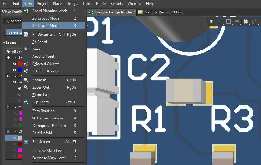
You can easily switch between the 2D and the 3D view in Altium Designer
Whether you are routing simpler 2-layer boards or complex HDI PCBs with high layer counts, Altium Designer® has the CAD features you need in an intuitive user interface. The huge set of hotkeys and automation features in Altium Designer help you stay productive as you build new designs. When you’ve finished your design, and you want to release files to your manufacturer, the Altium 365™ platform makes it easy to collaborate and share your projects.
We have only scratched the surface of what’s possible with Altium Designer on Altium 365. Start your free trial of Altium Designer + Altium 365 today.

About Author
Related Resources


Related Technical Documentation


Take advantage of the world's
most trusted PCB design system.
One interface. One data
model. Endless possibilities.
Effortlessly collaborate with
mechanical designers.
The world's most trusted
PCB design platform
Best in class interactive
routing
View License Options
Thank you, you are now subscribed to updates.