True ECAD / MCAD Co-Design Will Eliminate PCB Design Placement Errors
Table of Contents

Have you ever had a PCB design returned to you because a component that you placed conflicted with a mechanical feature? Missing even one conflict can cause a lot of grief when it comes time to install the circuit board into the final system. It certainly did in my case where that one part ended up in a location that ultimately wouldn’t fit in the device housing. The only way my layout would work was if I cut an opening in the enclosure for a large electrolytic capacitor.
PCB design is no longer a matter of laying out the board and then letting someone else worry about the rest, it takes true ECAD / MCAD co-design to get the job done quickly and correctly. Sadly though, a lot of PCB design systems are not up to this task, and designers still have to go through a laborious process of having their component placement verified through a system of reviews and prototype builds.
Fortunately, there are some PCB design tools that will allow you to do your own component placement to mechanical checking, and you can do this while you are still in layout. I have found that having this capability in my design tools has saved me a lot of time, cost, and embarrassment and I think that it could help a lot of other designers as well. Let me tell you more about what I mean.
Component Placement in Traditional PCB Design Tools is Painful
As PCB designers we are used to working with a lot of rules with our component placement. Working in different zones or regions on the board for optimum component functionality is second nature to us as we group components for signal integrity or power delivery. Working with mechanical constraints is a very different beast and it can cause pain with traditional PCB layout tools if they don’t display shapes in 3D.
PCB layout systems usually display components as a 2 ½ D shape, meaning that the component shape itself is in 2D with a maximum height property attached to it. This means that the entire component will be referenced at a single height even though there may only be a small portion of it that is actually that tall.
Take a right-angle D-Sub connector for instance. The board edge of the connector is the tallest part yet the entire component will be referenced at that height like a boxy cube. Without the ability to see the design in 3D, you can only work in 2D with a DRC notification if the maximum height property has been violated.
Traditional 2D PCB placement view relying on height properties for clearance checking
Traditional Placement Reviews and Prototype Builds are Slow and Expensive
For years, we were content to work within a 2 ½ D CAD environment (unless your capacitor sticks through the roof of your device – but let’s not bring up that painful memory again). Now, with the need for smaller boards to fit inside smaller devices for technologies like IoT, aerospace, and communications equipment, we need to work with tighter component placements than ever before.
A 2 ½ D design environment just doesn’t cut it anymore. An area on the board that should be OK to place a part could turn out to be a real violation because the part had a different contour than expected. Or the reverse may happen and you may move a component from its optimum position due to a 2 ½ D height violation only to find out that it would have in fact fit just fine where it was.
Adding to our problems as PCB designers are shrinking time and budget constraints. With design cycles getting shorter in order to meet time-to-market demands, there is less time and money for the reviews and prototype builds that we used to work with. Yes, you can still send your design files off to the mechanical engineering group and wait for them to get back to you on what components may be in violation.
This takes more time however and you may still have the same difficulties as before with them interpreting your 2 ½ D shapes. What you really need is to be able to see your shapes as well as the mechanical features that you are designing to all in the same 3D environment that you are doing the layout in. This way you can make immediate changes in your placement instead of waiting for someone else. The good news is, now you can.
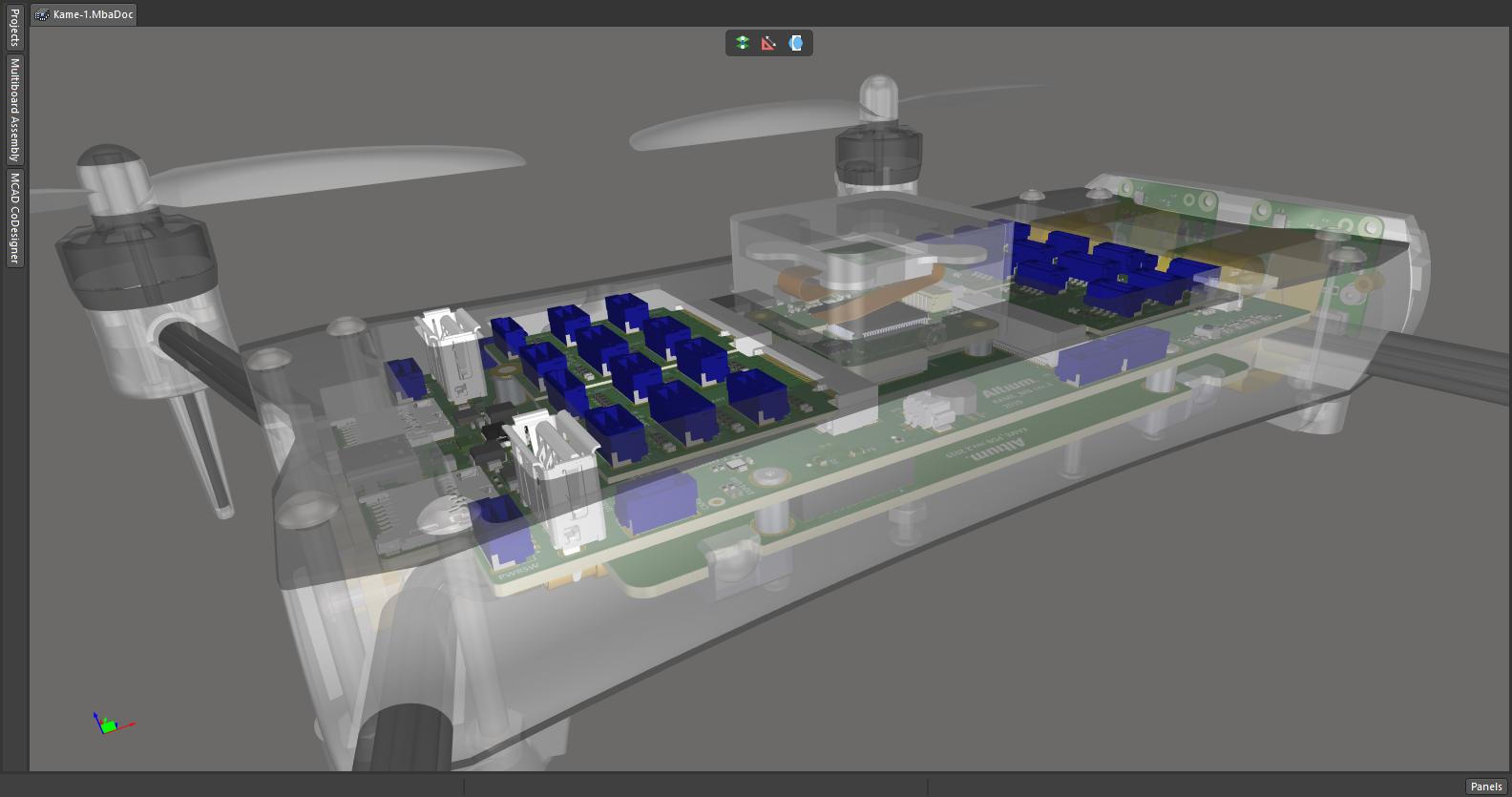
The same board placement in 3D giving you full true clearance checking
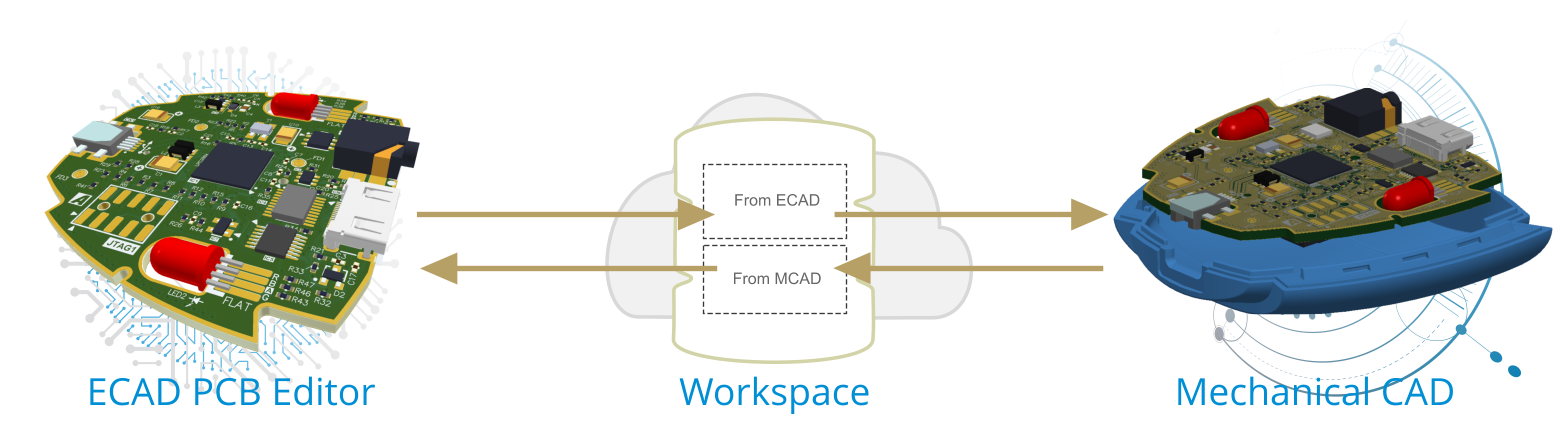
A True ECAD / MCAD Co-Design Workflow
The best PCB design tools today give you the ability to work within a 3D environment for placement verification and checking. To do this these tools will give you a variety of functions such as the ability to create 3D body objects either manually, or with auto-generation tools. You can also work with STEP models and exchange that data with MCAD systems.
With these capabilities, you will be able to import the mechanical CAD data and see immediately in 3D any component to mechanical feature placement violations and make the necessary changes. With functionality like this, you will truly be on your way to real ECAD / MCAD collaboration.
I have found that Altium Designer® is my tool of choice for the advanced 3D placement and MCAD features that we have been talking about here. Altium Designer gives me the ability to collaboratively co-design in order to reduce design iterations and initiate incremental design updates all within Altium Designer’s Native 3D™ engine.
With the ability to view and check my placement in 3D to the imported mechanical design files, I am able to get my designs done sooner and with a greater level of confidence that my components are placed where they should be for a successful design.
Altium is the PCB design software that has made a difference for us. Would you like to find out more about how Altium can help you to achieve a true ECAD and MCAD co-design workflow? Talk to an expert at Altium.
Start the journey to switch over to Altium Designer today.
Related Resources


Related Technical Documentation

Take advantage of the world's
most trusted PCB design system.
One interface. One data
model. Endless possibilities.
Effortlessly collaborate with
mechanical designers.
The world's most trusted
PCB design platform
Best in class interactive
routing
View License Options
Thank you, you are now subscribed to updates.
