Board Layer Stackup Considerations for High Speed Board Design

Table of Contents
High-speed designs will only operate successfully when they are built with the right PCB stackup. Your stackup must have the correct arrangement of power and ground planes, with enough layers allocated to signal, and all with material sets and copper selection that can be manufactured at the appropriate scale and cost. If a designer can get the stackup correct, then routing with ensured signal integrity is much easier, and many of the simpler EMI problems will be suppressed or prevented.
To help designers more quickly engineer and build high-speed stackups that support required routing and signal integrity, we've compiled important resources for different classes of high-speed stackups.
Low Layer Count Stackups
Simpler high-speed PCBs will start as 4-layer boards. My firm view is that 2-layer boards should not be used for designs that will support impedance-controlled high-speed digital interfaces because they cannot guarantee signal integrity or noise control. Any design professional will confirm this point.
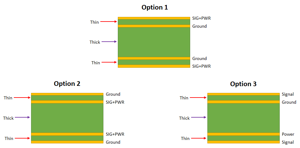
The three main types of 4-layer PCB stackups that can support high-speed signals are shown below. Among these stackups, Option 1 is arguably the best choice as provides the most flexibility in routing, and it can be used as a double-sided board. Option 2 can also be used for double-sided placement, but it limits where signals can be routed because there can be crosstalk in the internal layer. Option 3 is good if you have high power requirements, but you can only route high-speed signals on one layer; passives or mechanicals could still be placed on the back layer.
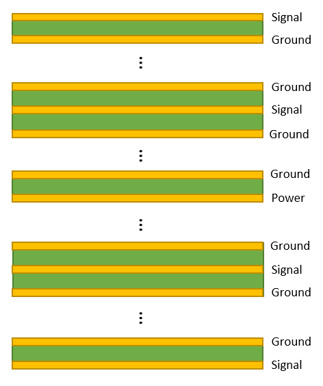
When higher signal counts are required, such as placing lower-speed signals in an internal layer, the next step is to extend Option 1 to higher layer counts. This would start with a 6-layer stackup, where a dedicated power layer and a signal layer are added into the stackup shown in Option 1 above. This stackup is useful for two reasons:
- Surface layers are good for controlled impedance high-speed interfaces
- Internal layers can support most slower interfaces or control signals
- The power layer can be broken into multiple large rails to support different core voltage levels.
The same procedure can be used to extend the stackup to 8 or more layers with high-speed signals; this type of PCB stackup is discussed in the next section.
Moderate Layer Counts
At some point, the board stackup can become so thick that the total PCB thickness will be larger than the standard value. In terms of manufacturing this is not a problem; standard lamination press processes can handle boards beyond the standard thickness value and reaching to multiple mm in thickness. If your goal is a thin board, then you will need thinner layers; options are reinforced PTFE laminates (discussed below) or moving directly to HDI processing.
Moderate layer count boards (above ~8 layers) can tend to have multiple planes layers allocated to power, as well as additional signal layes. For moderate layer count boards, there are few simple guidelines that can help suppress EMI and ensure power integrity:
- It's okay to divide up a power plane into multiple rails as long as signals are not referenced to that plane layer
- If there are multiple power planes, do not stack the power planes on adjacent layers; separate them with a GND plane
- Put fast signals on internal layers between two GND planes; do not reference these to power planes with any splits
- Only use the surface layers for fast microstrips, some power routing if needed, and some GND pour if needed
These guidelines might cause you to add a couple extra layers to your design, but the benefits will be much greater noise control, power integrity, and signal integrity.
More Advanced Stackups
The idea of "more advanced" in the context of high-speed PCB design could mean many things. In high-speed digital designs, it could have two possible meanings in terms of layer selection and arrangement:
- Thin layers to support HDI routing
- High layer counts that force the usage of thin layers
- Routing into fine-pitch BGAs on multiple layers (but not necessarily with HDI)
In other words, you could have very thin signal layers (e.g., 4 mils) with glass-reinforced FR4 with low layer count, or you could have very high layer counts that force the use of thin layers and possibly alternative materials.
The considerations in high-speed layer stackup design for these PCBs focus on required linewidths for components and manufacturability, not simply the Dk and Df values for a stackup. In some cases, a low-Dk, low-Df laminate is needed on signal layers, but not simply because losses are lower. In these designs, manufacturability and signal integrity reign supreme, and thin laminates can be the answer to many challenges in high-speed stackups with high-layer count and/or thin signal layers. Today's main option for thinner boards that can eliminate the need to move to the most advanced processing or HDI processing are reinforced PTFE laminates, which are available in thicknesses below 4 mils.
Other Resources
The other areas of stackup design that are important for high-speed PCBs are power integrity and signal integrity. There is also the potential need to shift to HDI designs when BGA packages have very fine pitch, and when layers get very thin. Take a look at these resources to learn more about these important areas of PCB design:
- 11 HDI Materials You Need to Know
- 2+N+2 PCB Stackup Design for HDI Boards
- Ebook: PDN Simulation and Analysis Guide
- The Impact of Stackup Design on Signal Integrity
When you need to specify materials, build a stackup, and perform impedance calculations to support high-speed PCBs, make sure you use the complete set of PCB design tools in Altium Designer®. When you’ve finished your design, and you want to release files to your manufacturer, the Altium 365™ platform makes it easy to collaborate and share your projects.
We have only scratched the surface of what’s possible with Altium Designer on Altium 365. Start your free trial of Altium Designer + Altium 365 today.

About Author
Related Resources


Related Technical Documentation


Take advantage of the world's
most trusted PCB design system.
One interface. One data
model. Endless possibilities.
Effortlessly collaborate with
mechanical designers.
The world's most trusted
PCB design platform
Best in class interactive
routing
View License Options
Thank you, you are now subscribed to updates.