4 Steps on How to Create a Component Footprint in Altium Designer

Table of Contents
When laying out your printed circuit board, it is critical that you know how to create footprint for your design components. Some components are quite common or they come in standardized packages, making footprints easy to find. In some cases, footprint generation may need to be done by yourself, and you’ll need to use information directly from the component’s datasheet. If the footprint is incorrect, the part pins may not align with PCB pads or the part may violate clearance or spacing rules that could lead to significant loss of time and additional cost.
When designing your PCB circuit board you can sometimes rely upon a program part to provide you with an accurate footprint for your part. However, this is not always the case and invariably you will at some point have to create your own footprints. With some PCB design software packages, this can be a difficult task that comes with a steep learning curve before you become proficient. With Altium Designer®, on the other hand, component footprint generation is quick with powerful CAD tools. Here's how to use Altium to create footprint for your design components.
How to Create a Component Footprint in Altium Designer
Component footprint generation is done in Altium Footprint Designer by following these 4 steps:
Let’s step through the process to see how easy it can be to create your component footprint.
Here’s how to create your footprint design in Altium Designer in 4 easy steps:
Step 1: Create the Pads
You will need the landing pattern for your part, which can be found towards the end of the component datasheet or in your chosen database library. For this example, let’s use the popular PIC24FJ64GA004 microcontroller. This component is packaged in a 44-lead plastic thin quad flatpack.

In Altium Footprint Designer, under File → New → Library → PCB Library. This will add a new PCB component footprint library to your project. You’ll also need to add new components to your PCB Library file. When you create a new PCB Library file, the library will create a blank footprint for your PCB layout (named PCBCOMPONENT_1) by default.
The first thing we need to do is set our units. Units are listed in the upper left corner of the window. The datasheet for the part only has dimensions in mm. If the dimensions given are in mil, then under the View menu click on Toggle Units to convert to mm.
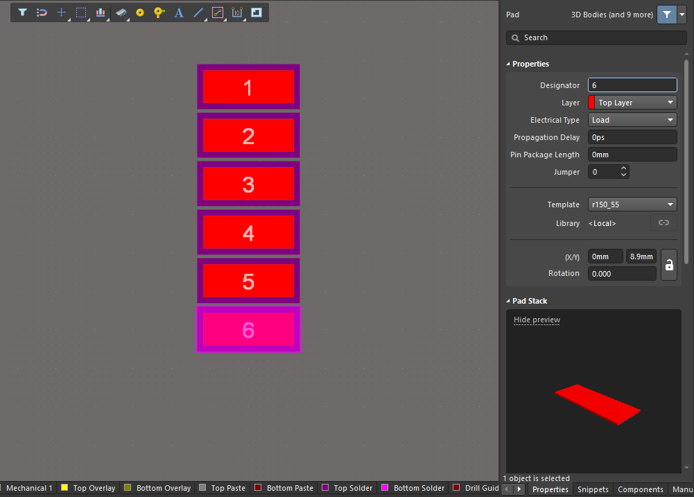
Click on the pad icon on the PCB Lib Placement toolbar at the top of the window (or click on Pad on the Place drop-down menu to get a pad. Place the pad near the middle of the window (we will set this in a moment). Now, right-click on the pad and select Properties. Next, scroll down to Size and Shape, set the shape to Rectangular, and the pad dimensions (X/Y) to 1.5 mm/0.55 mm. By default, the pad will be created as a pad with a plated through-hole. The hole will be removed once you select a single-layer pad template.
After you place a pad, there is some important information to enter in the Properties panel for each pad. First, you’ll need to set the designator number for each pad; this will link the pad number to the corresponding pin number in the schematic symbol. The next important point is the layer for this pad. Here, we are working with an SMT component, so we should select “Top Layer” from the layer dropdown menu. Each pad has an electrical type (Source, Load, or Terminator), and each pad has a propagation delay and pin-package length. All three pieces of information should be available in the component datasheet. This data is very important for simulations involving nets connected to these pads.
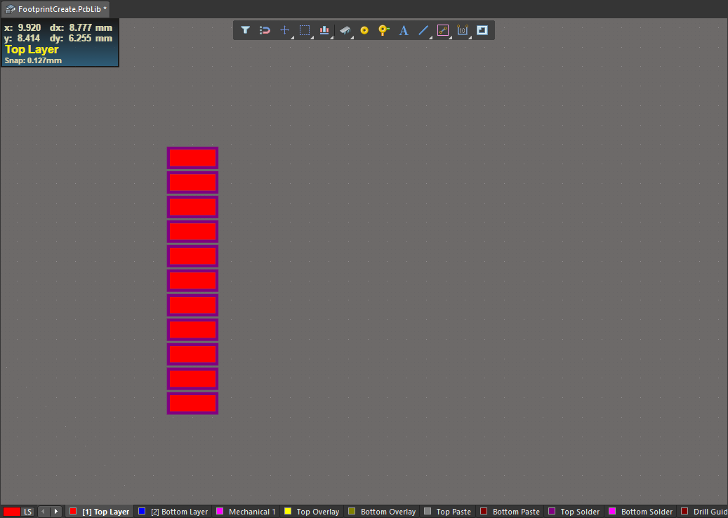
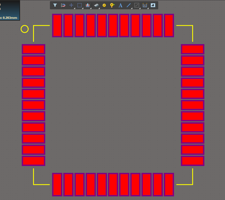
In the above image, I’ve placed the first 6 pads on the left side of the component. We can create an array of pads for each side of the layout by copying and pasting. (Tip: Select the pad(s) first then click on the Copy icon. To place, just click on the Paste icon.) We need to make sure that the distance between the pads is accurate. Here, the center-to-center distance is 0.8 mm.
One way to do this is to set the Global Snap to Grid value, which can be accessed from the View drop-down menu under Grids. Let’s use 0.2 mm, which means there should be 4 windows between the vertical centers. To make sure that the pads in our array are aligned accurately we select the array, then click on the Edit menu and select Align, then Align Vertical Centers.
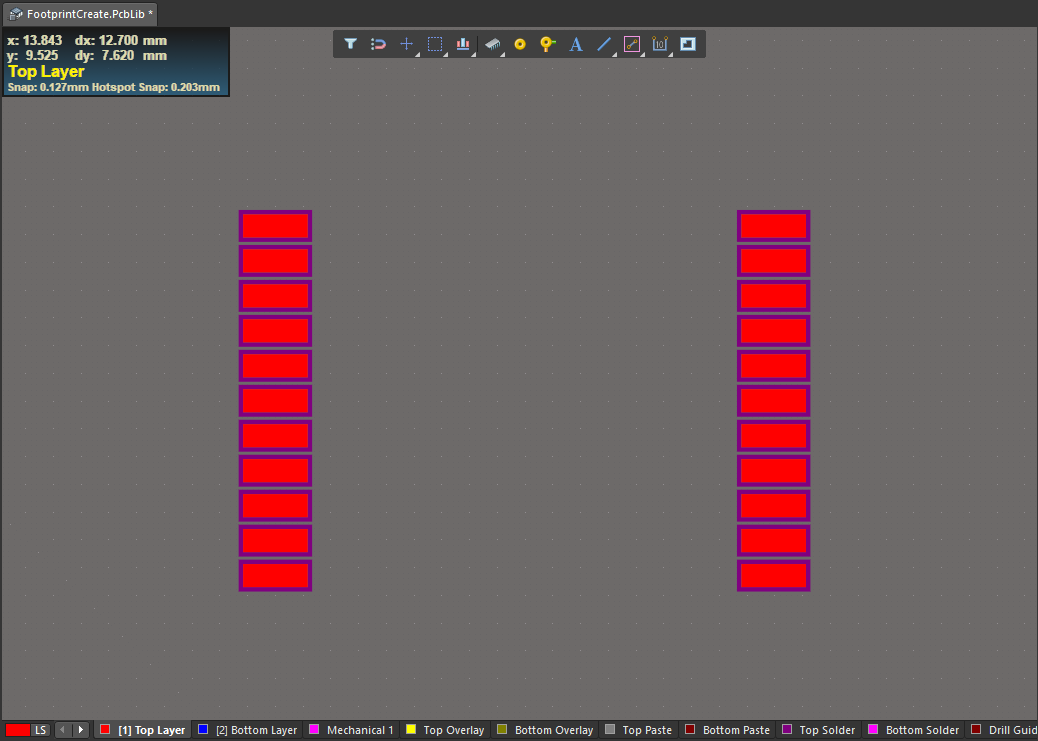
Be sure to follow the standard pin/pad numbering order when assigning designator numbers. Here, the pads are ordered counter-clockwise, with pad 1 placed in the top-left corner of the component. Next, we create the array for the opposite side by copying the array and pasting it 11.4 mm away at the same vertical level. Be sure to set the pad numbers for the new array.
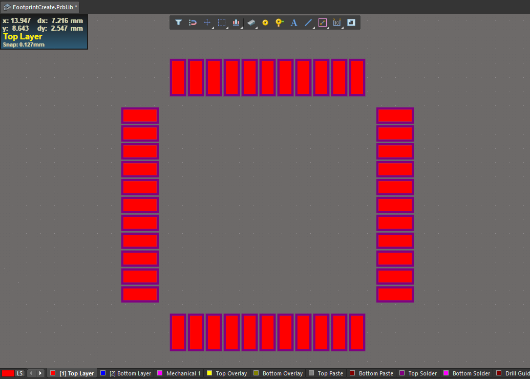
Now, we need to create the top and bottom pad arrays. Since our circuit component has a quad-flat package, the number of pins and dimensions for the top and bottom are the same. We can take advantage of this to easily create the other pin arrays by simply copying both left and right side arrays at once, pasting them, and rotating by 90°. Don’t forget to set the pad numbers in the Properties panel as you paste these new pads, otherwise, you will have duplicate designators in your PCB component footprint design.
Step 2: Define Component Height and Area
In this step, we need to define the height and area occupied by the component. We also need to define the component type. To access this information, select your new component footprint from the Footprints list, and click the Edit button. From here, you’ll be able to enter these three pieces of information.
By default, the component type will be set to Standard; this is the value we would want for this component. Other components, such as mechanical elements and no-BOM components, will not be standard components and should be assigned the appropriate component type. This window is shown below.
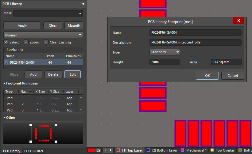
It’s a good idea to put the part number in the Name field; this is the value that will show when you import this component library into a different project. Put a useful description for the component in the Description field. Finally, the height and area can be found in the datasheets. For this component, the component height is 2 mm, and the total area is 144 sq. mm. This is shown in the package drawing below.

Step 3: Add Silk Screen Information
For this step, we add the silkscreen layer image and pin 1 marking. We will follow the suggestion from the data sheet and indicate only where the corners should be. To make a corner, we create a 0.08 mm line which you get by selecting the line icon on the PCB Lib Placement toolbar, duplicating it (by copying and pasting), and linking them. Here, make sure the silk screen information is assigned to the correct layer. Here, we want to place this on the Top Overlay layer. This can be done by selecting the silk screen lines from the Properties panel.
You will need to rotate one of these by 90°. To do so, click on the Edit drop-down menu, then Move, and then Rotate Selection. In the dialog, set the Rotation Angle (degrees) to 90. For the pin 1 marking, we will use a circle, which you can also select from the PCB Lib Placement toolbar. There is no need to make this too large, we only need this to be visible. (Tip: If you need to add labels or pin numbers, this is where you would add them).
The final step is to save your PCB Library file and your project files. You can then take your Schematic Library data and bundle it into an integrated library with your finished PCB footprint design so that it can be used in another project.
Step 4: Save the Footprint
The final step to create your component is to name and save it so you can add it to your component, which also includes the schematic symbol. Tip: You will want to make the name unique and searchable so you can easily locate it.
Additional Tips
The steps above illustrate a quick and easy way how to create a footprint for your components using Altium Designer software. Here are a few tips you may find helpful, as well.
- When you open the PCB window, check to see where the view is centered. You can determine this by looking at the dimensions as you move the cursor around. It is a good idea to center the view where you want the center of your component footprint design to be.
- If it is not on, you may want to make the grid visible. This is helpful to visualize distances. If necessary, you can set the grid dimensions by clicking on the grid icon on the top menu.
- Check to see if your component’s package already exists in the database of component libraries. To do this, click on the Panels tab at the bottom right then open the Libraries dialog. From here you can search the available component libraries with footprint designs.
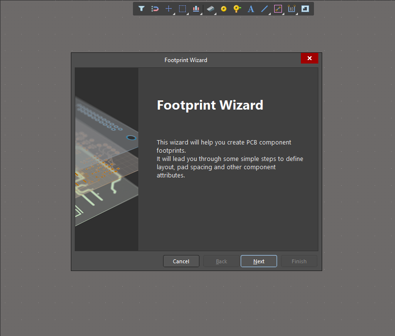
- If you would like a walk-through guide to help you with component footprint generation then try either the Footprint Wizard or the IPC Compliant Footprint Wizard. You can launch either of these from the Tools drop-down menu.
Footprint generation for your printed circuit board can be a painful process. Incorrect pad size, pad shape, or clearance can lead to a PCB layout that cannot be manufactured and require a redesign that will increase your product development time and cost. Altium Designer makes it simple to quickly create component footprint designs to prevent these issues. You can follow the four simple steps above or step through the process using one of Altium Designer’s PCB component wizards.
For more information on how to create footprint design for your PCB, contact an Altium Designer PCB design expert, or check out the Altium Designer Resource Hub for more information.

About Author
Related Resources


Related Technical Documentation


Take advantage of the world's
most trusted PCB design system.
One interface. One data
model. Endless possibilities.
Effortlessly collaborate with
mechanical designers.
The world's most trusted
PCB design platform
Best in class interactive
routing
View License Options
Thank you, you are now subscribed to updates.