Create Your PCBA Manufacturing Documentation with Draftsman

Table of Contents
In my numerous years in the electronics industry, we have come a long way. From using tape on mylars for PCB layouts to advanced CAD systems, the industry has moved what can only be described as light years ahead over the last 30 years or so. Gone are the days (thankfully) of a hand drawn schematic which is then translated by someone into physical that are connected by hand (even in early layout programs this was true). Netlist? What was one of those in a schematic? CAD tools have come along way since then, and using an advanced tool such as Altium Designer® can be a significant time saver in many tasks that are rarely (if ever) provided as automation tools in other CAD packages.
But I digress. This is the first of a series of two posts where I show how to perform important tasks of providing PCBA manufacturing documentation to contract manufacturers.
What's in Your PCBA Manufacturing Documentation?
So, let's suppose you have completed your PCB layout (or perhaps multiple printed circuit board projects). You are happy with the layout and you have generated the files necessary to get your latest work of art actually manufactured; but have you really generated everything your contract manufacturer needs?
I have seen a lot of data packs for manufacturing, from indifferent to great to, well, awful to be honest. With the advent of really fine pitch components in surface mount packages amongst other advances, the rules of manufacturing have changed as the older methods simply are not suitable for newer PCBAs. The manufacturing data package needs to provide arguably more guidance than was sufficient in the past.
What type of solder do you wish them to use? What are the reflow profile limits? These are two (of many) very important issues to make sure that the soldering process yields high quality joints. Solder joints are not the only thing to consider, though. As this series of posts will show, it is possible to convey very detailed information in a way that is clear and concise with no room for interpretation.
When you send out your design, you know what you want to have made, but the contract electronics manufacturer does not. They do not understand the design intent, where it will be used (which implies some steps that are not part of the usual CAD tool outputs) or how to test it unless you actually provide that information.
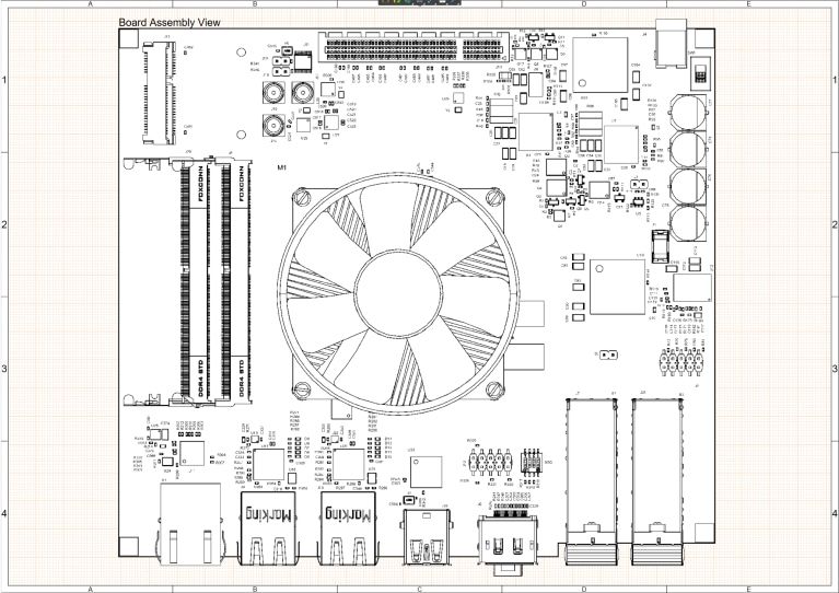
There are different types of packs depending on just what is being manufactured, so I will confine myself to the simplest for this post; the PCB assembly manufacturing pack encapsulated in the rectangle. This view is the assembly hierarchy and not how the outputs are actually generated.

The hierarchy shown is a typical setup for a PCBA manufacturing pack. Using the tools in Altium (from 16.1 onward), it is a breeze to generate a complete data package. Is it completely automated? No; every company and every design is different and there is some up front work to do.
Note that the pack shown is for a single assembly and could easily be a child or parent object to other higher or lower assemblies, making it ideally suited for companies with PDM (Product Data Management)/PLM (Product Lifecycle Management) systems. Let’s take a quick look at what is here:
Master Assembly Print
Not everything the manufacturer needs to know is in the electronic outputs (pick and place, BoM); there may well be special instructions, a test procedure to be used and other information. This is often missing from many packs, but it is not difficult to generate as we will see in a future post. This is the master drawing for assembly; everything else is subordinate. In the industries I have worked in, we call this a single source of truth. The schematic and BOM are standard outputs which generally already exist. I will take a look at how they can better support both internal teams and external manufacturing in a later post.
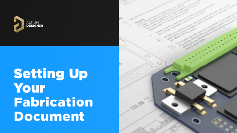
PCB Fabrication Master
This drawing, sometimes just called a PCB fabrication drawing, contains all the information a PCB fabricator needs to successfully make the bare circuit boards. The informating in this drawing may not be contained in the electronic design data, such as Gerbers and ODB++ files, although it is possible to generate a Gerber layer.
With complete information on the printed circuit board assembly, the contract manufacturer can generate a precise quote as they can properly estimate everything required; that means no surprises when a test is suddenly sent to the contract manufacturer who, apart from charging you for the test to be done, may need to put your assembly process on hold until operator time is available. Many contract manufacturers book their lines weeks and months ahead and organize their manpower and equipment accordingly. An incomplete pack can lead to a great deal of grief. Documentation and a single source of truth are key to a quality printed circuit board assembly process.
The PCB fabricator (often a separate company from the assembler) can generate an accurate quote as all the information they need is written down for them (my company template has 26 pre-defined comments for the PCB fabrication print).
Your data management team will adore you.
There is even a standard for these documents; IPC-D-325. By following this standard everyone understands what information is being conveyed.
I implemented this scheme at a company I worked for and a contract electronics assembler told me it was simply the best manufacturing pack they had ever seen. Wouldn’t you like to be able to show that email to your boss come evaluation time?
The bottom line: A complete fabrication pack can save time, money and schedule when done properly and there will be fewer questions and answers (although there should be some questions on a new assembly – no questions from the assembler and fabricator is a very bad sign).
When you need to quickly create PCBA manufacturing documentation for your design, use the Draftsman feature in Altium Designer®. Together with the OutJob file feature, you can quickly and easily generate manufacturing files without using a separate CAM application. When you’re ready to share your design outputs with collaborators or your manufacturer, you can share your completed design data through the Altium 365™ platform. Everything you need to design and produce advanced electronics can be found in one software package.
We have only scratched the surface of what is possible to do with Altium Designer on Altium 365. Start your free trial of Altium Designer + Altium 365 today.
About Author
Related Resources


Related Technical Documentation


Take advantage of the world's
most trusted PCB design system.
One interface. One data
model. Endless possibilities.
Effortlessly collaborate with
mechanical designers.
The world's most trusted
PCB design platform
Best in class interactive
routing
View License Options
Thank you, you are now subscribed to updates.