PCB Design Guide for Engineers: Part 2 — Planning
PCB Design Guide for Engineers Part 2 - Planning
The PCB Design Guide for Engineers is a series that serves as a guide for the novice/student, or electronics engineering professional. It presents a description of the methods, stages, and practices in producing a PCB from an engineer’s vision. From conception to delivery of the fully assembled PCB, this document takes you through basic design stages along with giving you proven industry practices that can be tailored to your organization's needs. In addition, useful links are provided for greater exploration of those topics.
INTRODUCTION
Planning the development of one or several PCBs can be a daunting task. There will be a host of other software tools that will be used in the development of your project. From tools that can be used to track the progress of your human resources within your team to the software tools used by your internal and external resources to bring your project to life. This PCB Design Guide for Engineers Part 2 - Planning will help you understand the Printed Circuit Board which is more important than the tool used to gather all of the data together intelligently to assemble the documentation required to bring to life the center of any electronic product.
THE TOOLS — USE A CENTRALIZED TOOL
There are a host of tools available that will most certainly allow you to complete your project and achieve your design goals. The difficulty when working with multiple tool sets is inherently getting these tools to communicate with one another for cohesive collaboration among all the people working on the project. Altium Designer® provides an all-in-one environment for developing your concept to simulation and signal integrity analysis. It gives you the ability to intelligently plan your board stack-up architecture and analyze and model your power distribution network’s (PDN) power integrity issues. Using real-time data from suppliers streamlines the generation of your bill of material. Altium Designer combines a powerful suite of tools that produce simple to complex multi-board projects.
SIGNAL INTEGRITY
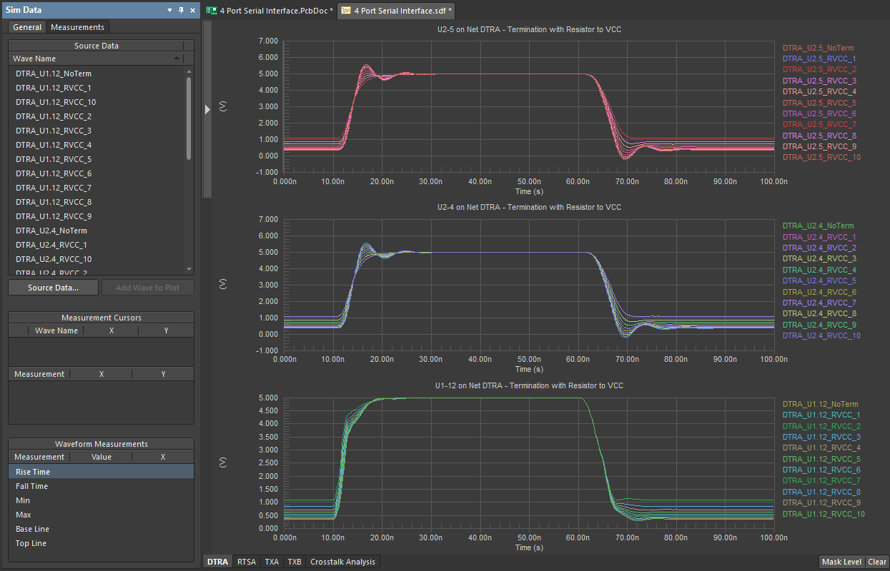
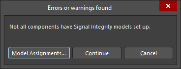
With Altium Designer, you can analyze the signal integrity (SI) performance of a PCB from either the schematic or the PCB editors, evaluate net screening results against predefined tests, perform reflection and crosstalk analysis on selected nets, and display and manipulate the waveforms.
Altium Designer includes pre-layout and post-layout SI analysis capabilities. The Signal Integrity Analyzer uses sophisticated transmission line calculations and I/O buffer macro-model information as input for simulations. Based on a fast reflection and crosstalk simulator model, the Signal Integrity Analyzer produces accurate simulations using industry-proven algorithms.
Preliminary impedance and reflection simulations can be run from your source schematics prior to the final board layout and routing. This allows you to address potential signal integrity issues, such as mismatched net impedances, before committing to board layout.
Full impedance, signal reflection, and crosstalk analysis can be run on your final board (or a partially routed board) to check the real-world performance of your design. Signal integrity screening is built into the Altium Designer design rules system, allowing you to check for signal integrity violations as part of the normal board design rule checking (DRC) process. If signal integrity issues are found, Altium Designer shows you the effects of various termination options, allowing you to find the best solution before modifying your design.
You can learn more about signal integrity using Altium Designer here: http://techdocs.altium.com/display/ASIAE/Performing+Signal+Integrity+Analyses
PRINTED CIRCUIT BOARD ARCHITECTURE
With Altium Designer, you have a robust set of tools that allows you to quickly and accurately produce the documentation that board fabricators require. It all begins with defining the characteristics of your PCB.
Board Planning
Altium Designer gives you the latest in board planning technology with three design modes. Beginning with Board Planning Mode, A two-dimensional design environment lets you define board regions and bending lines. A second 2D layout mode enhances the conventional two-dimensional design environment with customizable layer modes. A third environment provides a three-dimensional workspace providing vivid, realistic views of your PCB.
Here is further material relating to board planning:
- Board Planning Mode
- PLPCB~SetPCBViewModeEditOutline((Board+Planning+Mode))_AD
- Defining Board Regions and Bending Lines
- Board Shape
- Configuring and Working in 2D or 3D Layout Mode
- PCB 3D Projection Modes
Layer Stack Manager
The Layer Stack Manager helps you develop and model the physical and electrical characteristics of your PCB. From simple double-sided PCBs, and complex multilayers, to flex circuits and flex-rigid-flex designs. It also allows for variations and combinations of different materials and lets you define drill pair layers and specify bind and buried vias. You can enter your material characteristics and customize impedance formulas, allowing you to communicate a concise definition of your PCB through the various documentation media, generated by Altium Designer.
For more details on the Layer Stack Manager:
POWER DISTRIBUTION NETWORK (PDN)
PDN Analyzer is a DC power integrity (PI-DC) simulation tool that analyzes a board design’s DC performance based on its electrical and physical properties. DC analysis of a power delivery network (PDN), or the results of its DC power integrity (PI-DC), ensures that adequate copper has been provided in the path from the voltage sources to the loads, and the return paths. The result is an efficient design that maintains the integrity of the design’s DC power layout.
Learn more about the PDN analyzer from these sources:
BILL OF MATERIALS (BOM) ANALYSIS
Electronic projects can range from the simplest of boards to large-scale projects across a global enterprise, Altium provides several options that can be tailored to your organization’s specific needs and work seamlessly with your other tools to provide you with the information you need for the proper planning of your project.
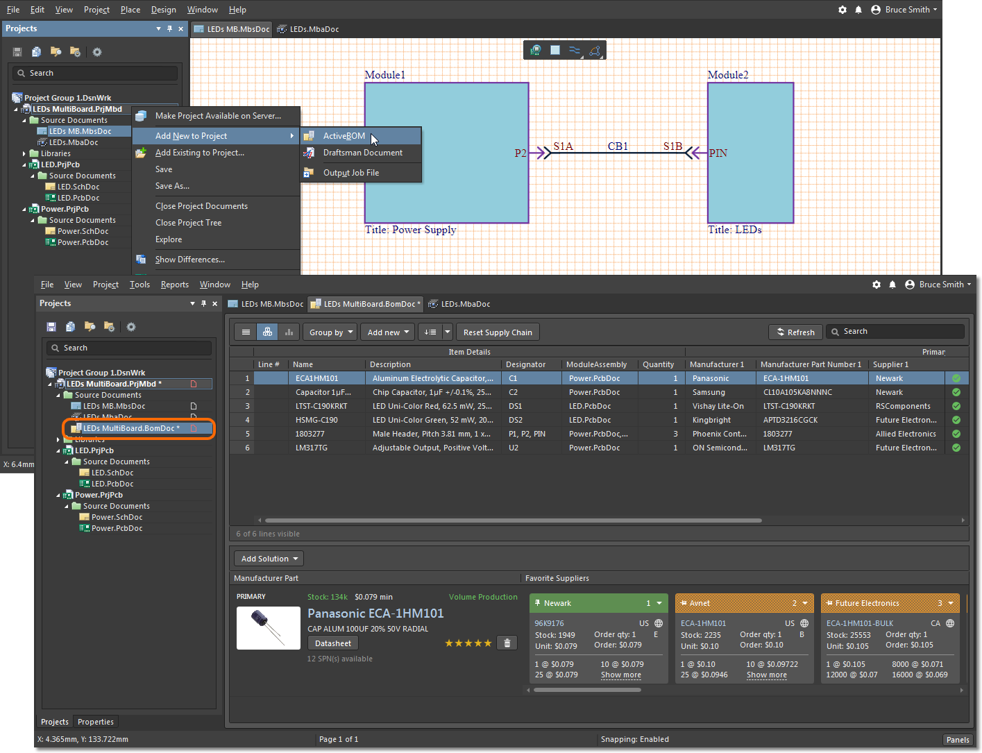
ActiveBOM
Facilitating real-time cost estimation and tracking for a board design, Altium Designer brings a system that effectively and efficiently aids the designer in managing costs and availability of items used in that design. This system is known simply as ActiveBOM.
ActiveBOM offers a live presentation of the design from the outset, providing early and ongoing cost estimation. It allows you to define target pricing at the individual item level. You can then track how actual costing fares against these estimates, and so give a timely flag if any cost blowouts are on the near horizon. In addition, you can quickly assess item availability, complete with a notification if there is a risk in the supply of a chosen part.
Download your free trial of Altium Designer and explore the features of our various bill of materials (BOM) analysis tools through our tutorials. In addition, here are more references for ActiveBOM:
ALTIUM VAULT
Altium Vault helps you to achieve your design goals by connecting all facets of the electronics design process together. Everyone involved in your design project can work without risking the integrity of your design data and without hindering their ability to remain innovative and productive.
By managing your components in the Vault, everyone involved in your design process has controlled access to all the relevant component data they need to ensure the best decisions are always being made. The Vault provides real-time supply chain data, component approvals, and life-cycle status information to the whole team. Designers, managers, procurement officers, manufacturing partners, and others involved in the design process are able to minimize errors, increase efficiency, reduce costs, and get products to market faster.
Learn more about Altium Vault:
- Request a Demo of the Altium Vault
- Getting Started with Altium Vaults
- The Altium Content Vault
- Altium Design Content
CIIVA
Producing an error-free BOM starts with staying on top of parts availability and pricing information from your most trusted suppliers.
SmartParts
Ciiva SmartParts Analysis allows you to instantly analyze all of your parts so you’ll never face another rejected BOM again.
- Ciiva SmartParts Search gives you all the information you need to find the right part for your designs including historical lifecycle data, verified alternative components, downloadable CAD models, and your own customized search history.
- Ciiva SmartParts Analysis allows you to produce a perfect BOM by instantly analyzing parts for current availability and pricing, with verified alternative part selections for any end-of-life components on your BOM.
- Ciiva SmartParts Management is seamlessly integrated into your PCB design environment to automatically store and manage all of your design and library data for you, so you can focus on what matters most.
Ciiva BOM Manager
From design conception to completion, you depend on your BOM to manage, track, and review every component used in your designs. The Ciiva BOM Manager enables you to automate your BOM management process in one centralized location.
- Stay in complete control of every change made to your BOMs with built-in version control. See exactly who made changes to your BOM and when, and understand exactly where your components are being used in every Bill of Materials.
- Easily swap out obsolete components with verified alternatives without ever leaving your BOM management tool. Get instant pricing and availability on every component and keep your production process running smoothly.
- Keep your entire production team on the same page with secure and centralized access to the same set of BOM data. Changes made by one person are instantly synchronized so you’re always working with the latest data.
Try it Free - Create Your Free Ciiva Account
CONCLUSION
Planning a PCB design project can be a complex and difficult task without the proper tools. The Altium Designer toolset allows for great flexibility in preparing and compiling your data with a shared and collaborative environment that will assure you the greatest success in completing your task meeting your scheduling needs and achieving your goals. Don't forget to check out PCB Design Guide for Engineers Part 1 - The Team.
Download your free trial of Altium Designer at https://www.altium.com/altium-designer-free-trial and explore the features of our signal integrity analysis tools through our tutorials.

 Open as PDF

