IPC-4761 Via Types
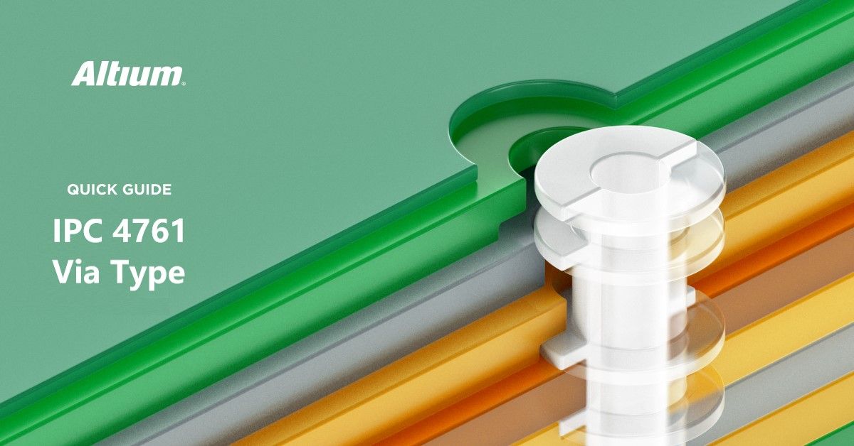
Table of Contents
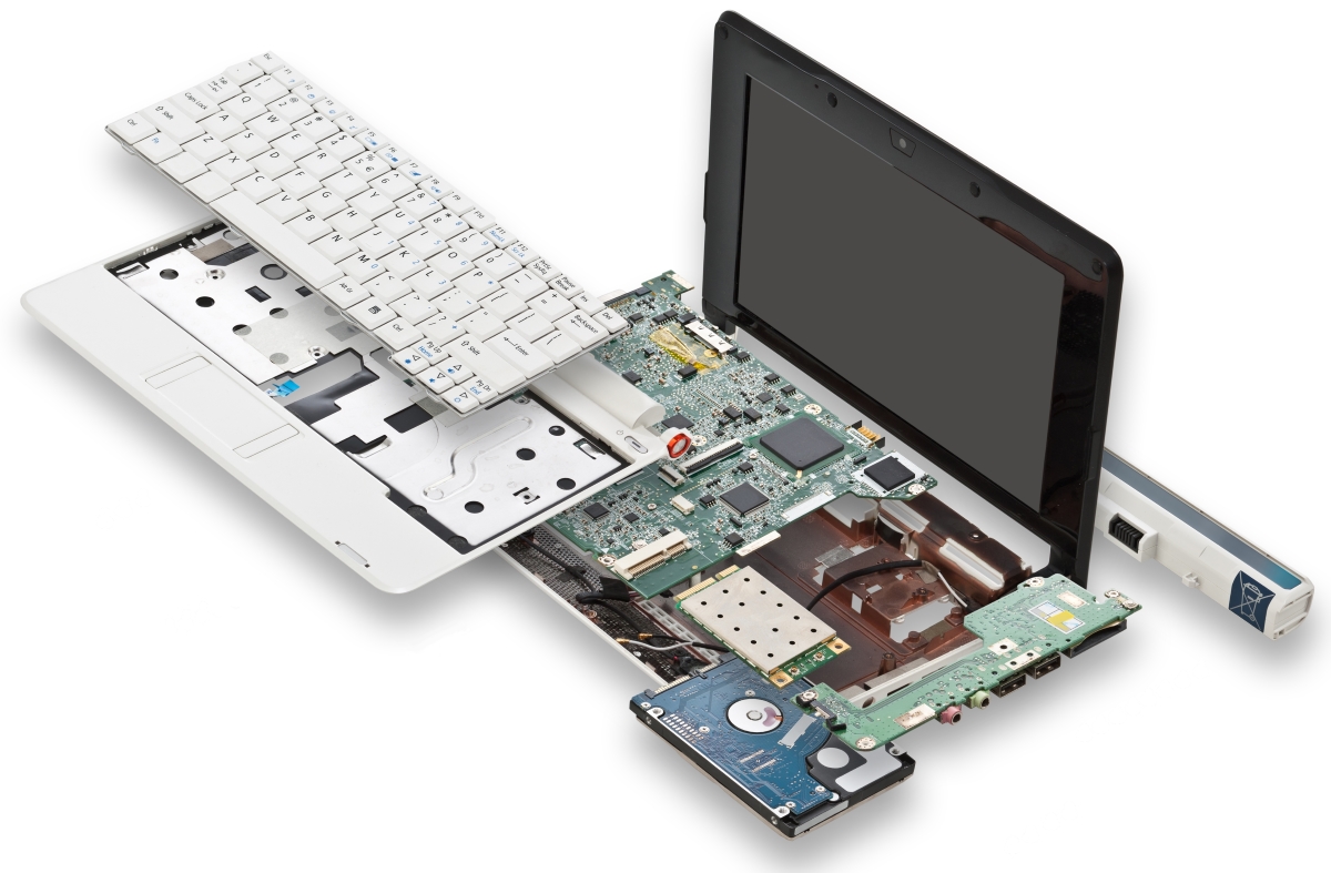
Via protection is an important part of modern PCB design. It provides additional benefits in PCB manufacturing and assembly, increasing the number of acceptable products. There are several types of vias protection detailed in the IPC-4761 Design Guide for Protection of Printed Board Via Structures and on pages 5-11 of this document.
Advantages of Via Protection
Common situations where vias protection is recommended or required:
Support For IPC-4761 Via Types in Altium Designer
Altium Designer supports vias types according to IPC-4761.
To configure the type of protection for vias:
- Select the desired vias;
- Set a type in the Properties panel;
- Specify the coating side and material in the table.
When a via type is set to IPC-4761, new types of mechanical layers and component layer pairs are automatically added to the design, with corresponding shapes on these layers.
The via protection types are also supported when creating output files for manufacturing, as well as when creating drawings in Draftsman.
Via Protection Definitions and Types
Tented Via (Type I Via) A via with a dry film mask material applied bridging over the via wherein no additional materials are in the hole. It may be applied to one side (Type I-a) or both sides (Type I-b) of the via structure.
Process: Vacuum laminated film material that is photo-definable.
Benefits: A consistent and repeatable process providing excellent hole tenting and uniform thickness.
Concerns: One side protection should not be used with bare copper hole walls! Chemical entrapment.
Concerns: Dimples may be a concern for adhesive processes where a glue dot is used for component placement.
Tented and Covered Via (Type II Via) A Type I via with a secondary covering of mask material applied over the tented via. The material may be applied to one side (Type II-a) or both sides (Type II-b) of the via structure.
Process: Application of mask over Type I.
Benefits: Improved tenting strength over Type I.
Concerns: One side protection should not be used with bare copper hole walls! Chemical entrapment.
Concerns: Bumps may be a concern in lifting the solder paste stencil. A conforming mask material is recommended to prevent significant increases in bump height.
Plugged Via (Type III Via) A via with material applied allowing partial penetration into the via. The plug material may be applied from either one side (Type III-a) or both sides (Type III-b) of the via structure.
Process: Screened and Roller Coated.
Benefits: Ease of processing. There are few manufacturing constraints.
Concerns: One side protection should not be used with bare copper hole walls! The plug material may protrude out one side of the via.
Concerns: Air expansion or even entrapped solvents can have a significant effect on plugs as they are being cured, causing «blow-out».
Plugged and Covered Via (Type IV Via) A Type III via with a secondary covering of material applied over the via. The plug and secondary covering material may be applied from either one side (Type IV-a) or both sides (Type IV-b) of the via structure.
Process: Application of mask over Type III.
Benefits: Increased plug strength. Pin holes that occur through the use of Type III plugging can be mitigated through the use of this type.
Concerns: One side protection should not be used with bare copper hole walls! Final finishes should be applied prior to plugging.
Concerns: Air expansion or entrapped solvents can have a significant effect on plugs as they are being cured, causing «blow-out».
Filled Via (Type V Via) A via with material applied into the via targeting a full penetration and encapsulation of the hole.
Process: Screened, roller-coated, or squeegeed.
Benefits: Complete fill of conductive or non-conductive material which eliminates contaminants. Process prevents solder balling. Benefits useful in sequential lamination processes.
Concerns: Voiding. The removal of excess material from the surface. Surface planarity. Complete curing. Excess process variables. Complexity of obtaining complete fill. CTE mismatch between the fill material and substrate.
Filled and Covered Via (Type VI Via) A Type V via with a secondary covering of material (liquid or dry film soldermask) applied over the via. The covering material may be applied from either one side (Type VI-a) or both sides (Type VI-b) of the via structure.
Process: Application of mask over Type V. Fill material can be electrically and/or thermally conductive depending on end use.
Benefits: Protection of the pad over Type V. The effects of surface voids possibly caused by using Type V method can be minimized with Type VI.
Concerns: Voiding. The removal of excess material from the surface. Surface planarity. Complete curing. Excess process variables. Complexity of obtaining complete fill. CTE mismatch between the fill material and substrate. Additional processing.
Filled and Capped Via (Type VII Via) A Type V via with a secondary metallized coating covering the via. Metallization is on both sides.
Process: Metallized coating over Type V. Applicable where high density features are required.
Benefits: Via-In-Pad and Ball-on-Via pad. Via stacking. Applicable where high density features are required. Benefits useful in sequential lamination processes.
Concerns: Adhesion of the metallized coating to the via fill and copper pad. Copper thickness. The planarity between the fill material and the copper surface. CTE mismatch between the fill material and metallization resulting in air gap (fill material shrinkage). Less than 100% via fill may result in a metallized cap that is too thin or a dimple that can also cause entrapped air resulting in voids in BGA solder joints. Pinholes in the metallized coatings result in non-solderable areas of a land where the capped via is intended for a BGA solder joint. Reduced solder volume is also a concern with dimples.
Via Type Definition in Exports
When one of these via types is implemented in a PCB layout, and it is time to export the manufacturing deliverables, these can be created in the Gerber configuration dialog or the ODB++ dialog. The IPC-4761 features that define the via types shown above can be exported as their own layers when creating Gerbers or an ODB++ export. These features are also automatically included in an IPC-2581 export should you choose to use this file format.
In Altium Designer, the IPC-4761 via features exports can be configured when preparing the Gerber export. This option will be automatically available whenever the PCB layout contains one of the IPC-4761 via types listed above.
Once these outputs are created, the via features can be viewed in a CAM editor in their own layer. This will allow the fabrication house to target filling/plugging and capping to a single region of the PCB if needed. Make sure to include a fabrication note that specifies the IPC-4761 via type requirement you need, including whether conductive or non-conductive fill is required in the fabricated PCB.
When you need to design your PCB vias and routing to ensure you comply with IPC-6012 Class 3 annular ring standards, use the padstack design and routing features in Altium Designer®. Once your design is ready for a thorough design review and manufacturing, your team can share and collaborate in real time through the Altium 365™ platform. Design teams can use Altium 365 to share manufacturing data, project files, and design reviews through a secure cloud platform and in Altium Designer.
We have only scratched the surface of what’s possible with Altium Designer on Altium 365. Start your free trial of Altium Designer + Altium 365 today.

 Open as PDF
