Buck Converter Simulation in Altium Designer

Table of Contents
Any new PCB you want to build will need a power source, and the power you need to provide is often stepped down from a noisier unregulated source. An example is an output from a full-wave rectifier, which will contain some residual ripple at the output port. Another possibility is the noise from an upstream converter. In other cases, you are drawing power from a battery, and the battery’s voltage/current output will change over time or with temperature.
No matter the situation, you can usually find a suitable DC-DC converter or LDO from a distributor, and you can easily add it to your board. When designing high power circuits (usually very high voltage and/or current), you’ll need to create a regulator from scratch and place it in your PCB layout. It's also the case that you may want to model a real component using discretes in a simulation in order to qualify the system's expected operating regime. As part of buck converter design, you can easily run a buck converter simulation directly in Altium Designer’s schematic editor. Here’s how you can access these features in the newest version of Altium Designer.
Starting a Buck Converter Simulation
The schematic editor in Altium Designer includes a SPICE-based engine for creating simulations directly from your design data. Other platforms provide similar tools, but they will eventually require you to export your design data and simulation data to an external program for analysis. Instead, you can do everything in Altium Designer, including immediately capturing your schematic as a new PCB layout.
After you’ve completed your buck converter circuit, you can access the schematic editor’s simulation tools in the new Simulation Dashboard feature in Altium Designer. You’ll need to complete the following steps to run a buck converter simulation for your circuit:
- Define your voltage/current sources. Simply use the Simulation Sources.IntLib component library in the Components panel to access a range of simulation sources. You need to simulate a DC input (or rectified AC input) and a PWM source for switching the high-side transistor (see below for more information).
- Place probes for desired measurements. The SPICE engine in Altium Designer will return current, power, and voltages for different nets and individual components. You can also place voltage, current, or power probes in your schematic to gather measurements on specific nodes or components.
- Create a simulation profile. With the schematic editor open, click on the “Simulate” button on the main menu bar. You can now access all the SPICE simulation features by clicking Edit MixedSim Profile. You can rename your profile as you like and configure a number of other settings.
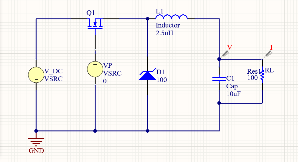
The image below shows a basic buck converter with a single NMOS transistor as the switching element and a diode as the rectifying element. The PWM signal is sourced from VP to provide the switching action in the MOSFET.
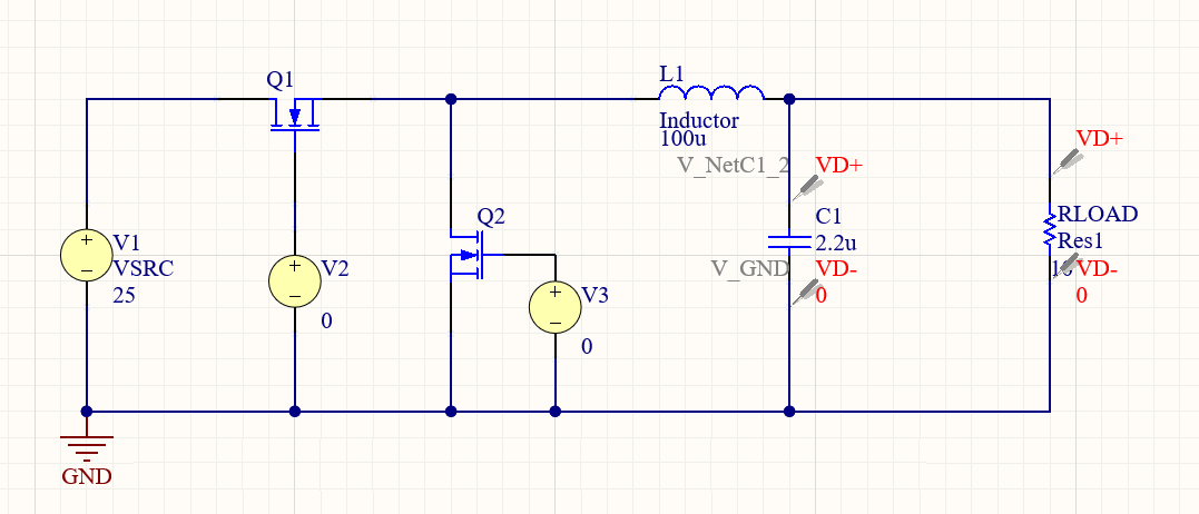
Case #1: A Synchronous Buck Converter With Two MOSFETs
A more complex buck converter topology uses two MOSFETs, one the same position as Q1 above, and the other as the rectifying element in replacement of D1. An example is shown in the schematic below. Q2 would be switched ON when Q1 is switched OFF, although the converter could still work with some dead time by driving the two MOSFETs out of phase with the same duty cycle. In either case, the same output voltage vs. duty cycle relation still applies. This type of buck converter is known as a synchronous buck converter.
The goal in a buck converter simulation is to examine how the duty cycle of the PWM signal, the load, and any other components affect the power output from your buck converter, and to verify that the output power demands can be met with the desired loadand operating parameters (input voltage and duty cycle). You should also examine ripple, ideally with an AC source and a rectifier bridge. It’s a good idea to start with the basic buck topology (see above) and add more features once you’ve chosen the right components.
Operation in Continuous Conduction Mode
The other points to examine the goals in a buck converter simulation include:
- Determine the minimum inductor size
- Determine if the operating frequency
- Determine the extent to which voltage drop across the MOSFET channels/diode reduces power output
- Verify the operating mode by examining the inductor current
Our intention in the above design is for the converter to operate in continuous conduction mode. In this mode, the inductor current never drops to zero and the output voltage will not be a function of inductor size.
The equation below relates the expected ripple currnet to the operating parameters in the buck converter simulation. For the desired ripple current, the required inductor size, PWM parameters, and input voltages should obey the equation below. Note that this is normally defined in terms of the voltage drop across the high-side MOSFET and the rectifying element (V(diode) in this case, could also be the low-side MOSFET):

If the converter is in the discontinuous mode, the output voltage will be a function of the inductance. If the converter is found to operate in the discontinuous mode in the steady state, then some of the operating parameters may need to change if the continuous conduction mode is desired. This would then allow one to implement a much more precise and simple control algorithm, such as you would find built into PMICs for gate drive control; the algorithm just adjusts the PWM signal based on the output to get highly precise power tracking and regulation.
- Learn more about continuous conduction mode in SMPS designs
- Learn more about selecting the PWM frequency for a power converter
Modeling the PWM Source
The PWM source can be modeled using a pulsed source. I’ve placed a voltage source in the above circuit diagram, and in building the simulation, you need to define that voltage source as a Pulse source in the Properties Panel. Here, we're using a generic NMOS power transistor model, so we will source a voltage from our PWM driver. The switching frequency and duty cycle of the PWM source can also be modified in the Properties Panel. Simply adjust the pulse width (duty cycle) and period (frequency) to tune your modeled PWM source (see the settings below). An example is shown below.

In our simulation, I’ve used slower 100 ns rising and falling pulse edges in the simulation settings with 30% duty cycle and 100 kHz frequency. This is sufficient for modeling purposes as these values are on the order of magnitude of what would be used in real buck converter circuits and PMICs. Also, because the pulse width and period are much larger than the rise/fall times, we would not expect these values to greatly affect the efficiency of the converter. However, in a real converter where the switching node has some parasitic inductance, the switching time can excite some transient that creates excessive high-frequency ripple on the switching node output voltage/current. If the rise/fall time were much slower, then we would need to include them as they become comparable to the pulse width and period.
The Simulation Dashboard
Once the PWM source is defined, you can use the Simulation Dashboard enable some analyses to perform in your simulation profile. Altium Designer's Simulation Dashboard is a central location where designers can configure mixed-signal simulations for their circuits inside the schematic editor. The Dashboard is accessible under the Simulate menu within the Schematic Editor. From here, you can run the four primary types of simulations you'll need for most circuits:
- Operating point calculation
- DC sweeps
- Transient analysis
- AC sweeps (a.k.a., frequency sweeps)
The Simulation Dashboard saves time as it will automatically check your design for simulation models and verify electrical rule checks. Custom output expressions can be added to display electrical measurements in your simulation results window. To learn more about the Simulation Dashboard, read the Altium Designer documentation. We can do everything we need in the time domain and adjust the circuit parameters to hit our required ripple and output.
Results
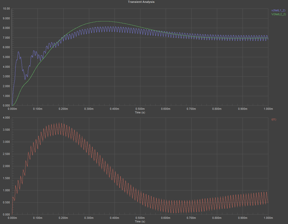
The image below shows the initial results with the converter as designed above, with output of 7 V when running at 30% duty cycle. As we can see, the converter exhibits a slow underdamped transient response with natural frequency of approximately 67 kHz as measured at the load. The issue here is that the overshoot might be excessive for this converter, reaching about 2 V during the transient response. The switching noise on the output is about +/- 200 mV.

The transient response is a bit excessive and the ripple is somewhat high. To improve the operation of this converter, one option is to include a filter on the output of the converter, but the filter needs to be carefully designed as it will add a new pole to the converter's forward transfer function.
Case #2: Buck Converter With Output Filter
The simplest filter design is to place an LC filter on the output to increase the rolloff in the transfer function. We then need to examine the transient response in the time domain. Note that we don't need to run something like pole-zero analysis to determine whether the new pole will create excessive transient response, we can see this directly from the time domain.
The modified buck converter design with the LC output filter is shown below.

The transient response of this filter is shown below. In this graph, we're comparing the filtered output (measured at C2) and the unfiltered output (measured at C1). Both graphs illustrate how the secondary filter stage adds a new pole to the transient response; the two transient responses are clearly overlaid on each other, exactly as we would expect in a coupled linear system. We still have approximately 2 V overshoot during the turn-on stage.

Case #3: Buck Converter With Output Filter and Capacitor ESR Included
In a real buck converter, the output capacitors will have some effective series resistance (ESR) that provides damping in the transient response from the converter, as well as the output filter. By adding in some damping, this slows the rise time and reduces the overshoot on the output voltage. A typical value for ESR values on capacitors used in power converters could range from 100 mOhm to 500 mOhm, depending on the type of capacitor and the package size, but capacitor manufacturers cannot always guarantee the expected ESR value for their components. If you're using controlled ESR capacitors, you'll have some guarantee on the specific ESR value, which is valuable if you are trying to control transient behavior on the output.
In the image below, we've included 1 Ohm in series with capacitors C1 and C2 in order to model the ESR value. It is also possible to intentionally place a small resistor in series to increase the damping; this is something you will see when you have multiple MOSFETs driven in series because the resistance helps prevent excessive ringing and overshoot that could damage the transistors.

The results below show how just a small amount of damping can be beneficial. This graph compares the three cases above (1 Ohm + filtered, filtered with no ESR, and no filter). We can see that the higher frequency transient response associated with the L2-C2 stage (our LC filter) is attenuated. You can calculate using basic RLC circuit theory whether or not this has been brought into the overdamped state. However, we still have significant overshoot in the output voltage due to the transient response from the L1-C1 stage.

Case #4: Buck Converter With Output Filter, Capacitor ESR, and Larger Capacitance
The last case we'll examine is to see how increasing the output capacitance affects the output voltage. This is another common design choice as capacitance on the output is generally seen as a filtration mechanism for high-frequency noise. We now want to examine whether this will work in the above design. The schematic below shows the circuit above from Case #3, but with larger capacitance on the output.

Now with this much larger capacitance on the output stage, we can see the effects of this filtration on the transient response when we measure at the output of L1, and at the output of L2. The results are quite interesting, revealing a long turn-on time with somewhat lower overshoot seen at the load. The ripple on the output is greatly suppressed and is almost unnoticeable in this scale. The slow transient response is also mirrored on to the inductor current, which almost enters discontinuous conduction mode during the turn-on stage. Therefore, we would not want to add in any more capacitance if we wanted to ensure the converter is always operating in the continuous conduction mode, even throughout its turn-on phase.
Next Steps
If you’re happy with your power converter circuit and you’re ready to interface it with the rest of your system, you can take a few paths:
- Select real components with same operating parameters. Typically you would select components, run a simulation, and then update your component choice based on simulation results. Once a component topology and external passives have been qualified, the real component can be placed in your schematics.
- Integrate your circuit into hierarchical schematics. If you have a higher level schematic, you can bring the converter into a larger system using the hierarchical design features in Altium Designer. Click here to see how this works for complex systems.
- Create a PCB layout. If the converter will operate on its own, all you need to do is use the integrated schematic capture tool to create your layout. Click here for a guide on creating a new layout from your schematic.
When you’re ready to layout your new board, you’ll simply create a PCB and use the integrated schematic capture tool to import your components into a new layout. You can now start arranging your components in your new layout.
If you’re familiar with switching converters, you know they can create significant noise in your circuits. The basic mechanism is due to a strong magnetic field during switching in the FET, which then induces a current somewhere else in the circuit. The second mechanism is a ripple problem, which can propagate through the converter and appear as noise on the output. EMI induced anywhere in your buck converter circuit, whether through switching noise or an external EMI source, can appear on the output signal if the output stage is not filtered. You can read more about suppressing noise from switching converters in this article.
Share Your Simulation Models and Schematics in the Cloud
If you're collaborating with other designers on a buck converter simulation, you can use the complete set of sharing tools in Altium 365 to store and access simulation models for your components and simulation models. You can share your schematic sheets as individual files or in a project so that others can access your simulations. You can also share individual .subckt models for specific components in a cloud environment. You can also access your .subckt models when creating a new component. All of this can be instantly imported into Altium Designer without manually downloading and organizing your simulation files.

The above image shows the web interface for Altium 365, where users can organize and store their simulation files for components in a secure cloud platform. SPICE simulation models can be stored along with footprints and symbols, and sourcing data can be attached to real components to help speed up procurement. Read this recent article to learn more about sharing your SPICE simulation models in Altium 365.
When you need access to the world’s best circuit design, simulation, and PCB layout tools, try using the full suite of design features in Altium Designer®. You’ll have everything you need to create a new board for your DC-DC converter, run a buck converter simulation, and find your board's components. The Manufacturer Part Search feature allows you to source the component models you need for your design direct from major distributors and component manufacturers.
We have only scratched the surface of what’s possible with Altium Designer on Altium 365. Start your free trial of Altium Designer + Altium 365 today.

About Author
Related Resources


Related Technical Documentation


Take advantage of the world's
most trusted PCB design system.
One interface. One data
model. Endless possibilities.
Effortlessly collaborate with
mechanical designers.
The world's most trusted
PCB design platform
Best in class interactive
routing
View License Options
Thank you, you are now subscribed to updates.