Decoding PCB Fabrication Notes

Table of Contents
Sending a board out for fabrication is an exciting and nerve-wracking moment. Many sleepless nights have resulted from an initial fabrication run, and it’s important to ensure everything is reviewed, re-reviewed, and can pass a DFM inspection! If you need to get a design into fabrication, one of the important pieces of documentation you can create is a fabrication drawing. Inside this drawing, you’ll need to include PCB fabrication notes that tell your fabricator how to build your board.
Why not just give your fabricator your design files and let them figure it out? There are a few reasons for this, but it means the responsibility comes back to you as the designer to produce manufacturing files and documentation for your PCB. In addition, if someone sends you a drawing for a design, you should at least be able to read the drawing and understand what it’s saying. If you’ve never needed to place information into a fabrication drawing or prepare fabrication notes, it’s actually quite simple if you have the right design tools. We’ll look at how you can do this inside your PCB layout and how this will help you quickly generate data for your manufacturer.
What Are PCB Fabrication Notes?
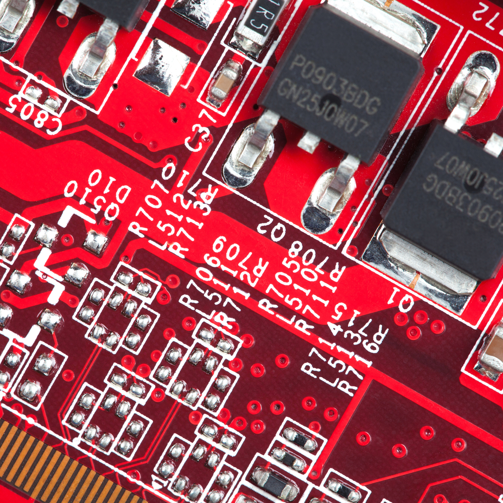
A PCB fabrication drawing is used by a manufacturer to make sure everyone on the shop floor understands the requirements of a given design and how that design should be fabricated. Within a fabrication drawing are PCB fabrication notes. These notes are generally templatized by different design or fabrication houses as there is no strict standard that indicates what should or should not be included in PCB fabrication notes. Your notes are not literally telling your fabricator how to build a PCB, they are there to tell the fabricator the requirements in the final bare board so that the overall build can be successful.
This means that, when you’re preparing to send a design in for manufacturing, you don’t need to manually rewrite all the fabrication notes: you can copy your template into your PCB layout, insert some of the important points that are design-specific, and send that over to your fabricator for review. Just as an example of what you’ll see in PCB fabrication notes, take a look at the example below.

If you want to open a text-based copy of the above notes and adapt them to your projects, you can get them from this link. Your notes can be put into a format that is shorter or more convenient for your projects. If you’re an individual designer and you work on a lot of projects, placing these notes in the PCB layout or in a fabrication drawing can help you keep track of project requirements. If you’re working at a larger organization, you probably have specific requirements from your employer. If these requirements aren’t specified, then it will be up to you as a designer to come up with these.
PCB fab notes aren’t strictly standardized in terms of content and format. However, there is some basic information that you’ll find in any professional set of PCB fab notes, and some of this information is self-explanatory. Something like board thickness or tolerances are (or should be) rather obvious. Other aspects of fabrication notes deserve some explaining. I won’t get into every point in the above example, but I do want to highlight a few of these as they are critical for ensuring your board is fabricated correctly.
Note 1: IPC Class Level
This note specifies the performance level of the board when deployed in the field according to the IPC-6012 standard. This is a reliability standard, and your fabricator will use this to determine the level of inspection they need to perform to ensure reliability. The three classes are:
- Class 1: Reserved for throw-away products intended for one-time or few-time uses
- Class 2: Intended for products with extended lifetime that will be placed in continuous service
- Class 3: Intended for the highest-reliability products where human life may be at stake should the product fail. This is a standard requirement for military, medical, and aerospace equipment.
Typically, if you do not specify this, the default inspection level will be Class 2, or possibly Class 1 if you’re going with a budget fabricator. Some designs or fabricators can only conform to IPC-A-600 inspection levels; I’ll discuss these differences in an upcoming blog.
Note 4-6: Surface Features
All surface features should be specified, including solder mask, silkscreen, and plating. If you don’t specify these, you’ll usually end up with tin-lead or silver surface finish, so make sure to specify something more reliable like ENIG if you need it. For the silkscreen font and size, you don’t need to include that here, that will be shown in your Gerbers.
Note 15: Testing Requirements
The above example shows a flatness requirement for the board, but what it’s really doing is listing a testing requirement. Note that Part B of Note 15 lists:
- TEST IN ACCORDANCE WITH THE CURRENT REVISION OF IPC-TM-650 2.4.22
The IPC-TM-650 2.4.22 is a specific test method to which the bare board must conform. This is a standard requirement to ensure components are not tilted during soldering and assembly.
Other testing requirements could be listed in this section. Such requirements could include drop or delamination testing, vibration testing (normally used in the PCBA), oxidation testing, temperature cycling testing, or any other tests that you deem important in your end application. If an IPC standard or other industry standard lists the methodology required for the test, then that standard should be listed along with the specification the board needs to meet. This is common in mil-aero boards that have specific safety or reliability requirements beyond those specified in the IPC standards. If this is a hobby project or a one-time prototype run, you typically don’t need to specify anything beyond flatness, which is a standard performance requirement among fabricators.
Note 16: PCB Material
I’ve looked at the importance of your materials and how to specify materials in an earlier blog post. This section should specify the most important requirements of your material. The flammability rating in the above example is the standard NEMA rating that is used to define what is an FR4 substrate. The other note (part B in the example) is the glass transition temperature (Tg) value. The higher the expected operating temperature of your board, the higher the required Tg value for the substrate, which ensures the PCBA can withstand thermal cycling. In this section, you shouldn’t specify the dielectric constant requirements; that gets covered under the impedance section.
Note 17: Registration Tolerance
The registration level in your board refers to the horizontal misalignment between layers in the PCB. When the PCB is pressed, there will be minor variations in the lateral alignment of the layers, usually less than a couple mils. You can never get this number to 0 mils, but fabricators will generally get close enough that you won’t have to worry too much about mis-registration when drilling and plating vias. Low misalignment ensures that any pads placed on through-hole vias will line up and make a strong connection to the via barrel.
In IPC Class 3 designs, you’ll likely need to add a teardrop to ensure a strong connection to the via in case there is any misregistration and breakout. Make sure your PCB routing tools can apply teardrops if you’re designing to this level of reliability.
Note 19: Impedance
Impedance can be tricky as it relates closely to the PCB material requirements. The reason we want to specify Tg and flammability in Note 16 is that these values can apply across a range of different materials. However, not all of those applicable materials will give you exactly the right impedance, so the impedance you specify may only be possible with a few specific materials that can fit into your stackup.
There are a few ways you can go about setting your impedance requirements in your design:
- Specify width and spacing: You can specify the impedance values you need for single traces or differential pairs on different layers, as well as the width required, as I’ve done in the example. Note that not all fabricators can or will select materials to meet these goals for you; some fabricators simply don’t keep enough materials in stock to mix and match laminates to hit your goals, and you’ll have to go elsewhere or pay extra.
- Use your fabricator’s stackup: The better route is to just call your fabricator, get their standard stackup for your layer count, and use their trace width/pair spacing values for your board to ensure controlled impedance. This way, you’ll know they can fabricate your board as you’ve designed it. You’re not required to do this, but when you go to higher layer counts, the extent of any redesign required to meet impedance requirements will be greater, so it’s best to just ask for this information before starting the design.
If you have multiple requirements you need to specify on different layers, you can create an impedance table that includes width and reference plane information on each layer in your PCB fabrication drawing. You could then include the text "SEE IMPEDANCE TABLE FOR WIDTH AND TOLERANCE REQUIREMENTS" (or write something similar).

Where Should You Put Your PCB Fabrication Notes?
Notes should be placed in the fabrication drawing, such as in a DWG/DXF file or in a PDF file. The board fab drawing, drill table, impedance table, and stackup drawing might all be on the same page, and you can certainly put the notes on this page if there is room. It’s common to place the drill drawing, stackup drawing, drill table and notes on one page, and then place the Gerber layers on a different page.
The other option that is popular is to put them directly in the PCB layout, meaning you basically turn your PCB layout into a big PCB fab drawing. Use a String object in your PCB layout, and just paste the fabrication notes directly. They can be placed on a mechanical layer and exported as part of your Gerbers (you can place it in the Drill Drawing layer). This lets anyone who has your project file see the fabrication notes directly next to the layout.
Call Your Fabricator Early to Ensure Success
The best route you can follow when building a new board is to call the fabricator early and find out what needs to be in your PCB fabrication notes. If you can get this data early, you can include it in your PCB fabrication notes with your fab drawing. This document will be the central repository for your project’s design data, so it’s good to keep thorough fabrication notes for the design should you ever plan to produce it again in the future. Keeping documentation is also good for individual designers that want to make the transition to working in larger organizations, where documentation is much more critical and needs to be very thorough.
Before you prepare your PCB fabrication notes, you’ll need to create your PCB layout with high-quality, easy-to-use software like CircuitMaker. Users can easily create new projects and make a smooth transition into manufacturing. All CircuitMaker users also have access to a personal workspace on the Altium 365 platform, where they can upload and store design data in the cloud, and easily view projects via a web browser in a secure platform.
Start using CircuitMaker today and stay tuned for the new CircuitMaker Pro from Altium.

About Author
Related Resources


Related Technical Documentation

Take advantage of the world's
most trusted PCB design system.
One interface. One data
model. Endless possibilities.
Effortlessly collaborate with
mechanical designers.
The world's most trusted
PCB design platform
Best in class interactive
routing
View License Options
Thank you, you are now subscribed to updates.