Design for Manual Prototyping and Throw Off Your Restraints
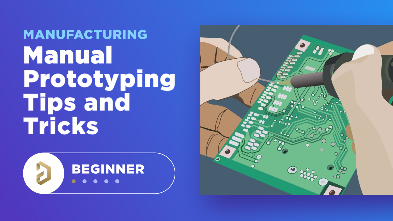
Table of Contents
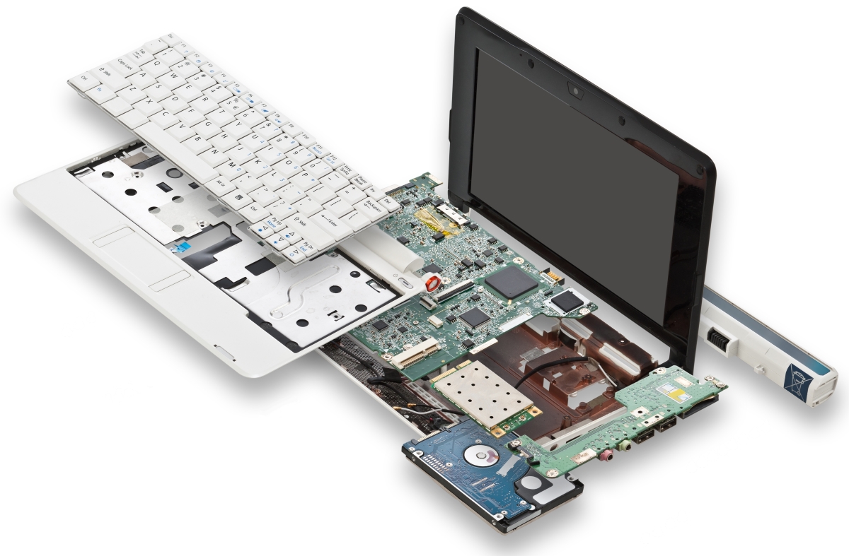
The term "manual prototyping" can mean a few different things. It could refer to at-home fabrication and assembly of a PCB, cobbling together modules into a small system, or just manual assembly of a simple prototype. If you're building one of your first designs, it is possible you would want to go through the assembly process by hand. Even further, some novice designers will want to etch their own boards with an at-home ferric chloride solution.
Generally, the choice to do any manual prototyping for a PCB comes down to cost. It is true that doing things on your own reduces the cost in terms of money, but it requires time and effort to assemble something correctly. Whatever you choose to do with your prototypes, there are some simple steps to ensure you get the greatest benefit from the time you spend manually building your prototypes.
Useful Tips When Designing for Manual Prototyping
The tips outlined below should help ensure your prototype design can be easily assembled and configured once you have placed all components.
1. Get the Right Equipment
First things first, you need the right equipment if you want to hand solder anything to your prototype PCB. Manual assembly with a soldering iron or with a hot air gun are both suitable options, or you can go the Mark Harris route and build your own reflow oven. Here's a short shopping list:
- Hand soldering iron station with multiple tips (such as JBC or Weller)
- Hot air gun for SMT or rework
- Solder wire and solder paste
- Solder flux, either dispersible in a syringe or in a pen
- Desoldering wick for rework
- Cleaning agent (rubbing alcohol)
- A good set of tweezers for small SMD components
This is not an exhaustive list of what you'll need in your lab, but it's what you'll need to start manually assembling your boards.
2. Use the Right SMD Component Size for Passives
Many manual prototypes will only use through-hole components as they are easy to handle and assemble by hand. However, if you want to do anything with a more modern digital components, you must use SMD components as these are standard packaging for more advanced devices. You will also find many connectors, passives, and power components available as SMD components.
For passives, SMD passives are available in multiple sizes, with the smallest being 0201 (20 mil by 10 mil) and 2512 being the largest. 0201 passives are very difficult to solder manually, and don't be surprised if you happen to mysteriously lose some of these components behind your lab bench. Also, smaller SMD components are very easy to mix up; don't be surprised if you accidentally swap SMD chip resistors with the same case size but different resistor values.
Don’t go too small in size.
I think it's worth taking some time to see what SMD passive sizes you are comfortable placing and soldering by hand. As your SMD components get smaller, you won't have the luxury of using your iron to solder these simply because they are too small; you're better off using hot air. If you must use a soldering iron, then it's a good idea to make your SMD pads longer so that you can reach them with a solder wire and iron.
3. Avoid Ball Grid Array (BGA) Packages, If Possible
Soldering tiny pitch components like QFPs or TSOPs can be difficult, but it is certainly possible with an iron, and it is much easier with hot air or a small oven/hot plate. BGA packages can't be soldered with an iron simply because you won't have a way to reach all the pads underneath the component. Instead you will have to use hot air for these components.
The other problem with BGAs in manual prototyping is inspection. These components are normally inspected with an X-ray inspection system as this allows direct visualization of the balls beneath the BGA package. If there happens to be a problem with the prototype, it will be more difficult to diagnose whether the problem is due to an assembly defect or due to some other problem in the system.
BGA package - not the friendliest for manual prototyping.
That being said, you can still probe the BGA connections from the back side of the board as long as you use through-holes for the BGA fanout. Make sure you do not tent the back layer if you want to access those BGA connections with a multimeter probe as part of your insepction. This is one way you can check for bridged pads in your BGA, although it will take a lot of time due to the high number of connections typically found on a BGA. For these reasons, it might be best to avoid BGAs in your prototype board and go with an alternative leaded package like QFP.
4. Use Thermal Reliefs
There will be pads where you try to apply solder and form a joint with an iron or a heat gun. The problem is that the board may not have uniform temperature across the board, and heat will leave pads if they are connected to a plane or large copper pour region. The result is that the iron or heat gun may need to be brought to a very high temperature just to solder a single pad, and this will risk damaging the board or components.
If you don't have a good hot plate for soldering or an oven, this can be prevented through use of thermal reliefs. Placing thermal reliefs on certain pads will help prevent heat migration into large copper regions, so you will be able to more easily form a solder joint on the component at lower applied temperature.
5. Make Use of Testpoints, Jumpers, and Solder Bridges
The point of many prototypes is to test as many functions of your board as possible. This means you will want to make some parts of your PCB layout configurable. One way to do this is to use test points, solder bridges, and jumpers. These components allow you to make or break connections, probe electrical values, take measurements, and even measure signals with an oscilloscope. With a properly sized solder bridge in the PCB layout, you can even solder small SMD chip components into signal lines as needed.

6. Breakout Extra I/Os to Pin Headers
The other part of building a prototype is making connections with other systems, or accessing I/Os to connector to other development products. This is why it is a good idea to bring all your extra I/Os to pin headers. With access to your I/Os to pin headers, you can do application-based prototyping as well as board-based prototyping. You can also connect to external components like sensors, small motors, LEDs, buttons, programming modules, or anything else you can think of. These will generally be low-speed I/Os, so you can use a simple through-hole pin header to make these connections. I recommend putting a 22 Ohm SMD resistor on incoming I/O lines near the pin header to slightly slow down these signals as this will reduce EMI.

When you need PCB design software that scales down to small feature sizes and helps you prepare a high-quality prototype circuit board for manual assembly, use the complete set of CAD features in Altium Designer®. When you’ve finished your design, and you want to release files to your manufacturer, the Altium 365™ platform makes it easy to collaborate and share your projects.
We have only scratched the surface of what’s possible with Altium Designer on Altium 365. Start your free trial of Altium Designer + Altium 365 today.


