PCB Ground Plane Design in High Performance Boards

Table of Contents
I sometimes see questions from young designers about how to design a ground plane into a PCB. A ground plane, or even grounded copper pour, is probably the simplest structure you will ever design in a PCB. What matters is what you can do around the ground plane in terms of placement, routing, and fabrication. Another aspect that often comes up is whether it is appropriate to create two different ground regions in the same PCB and thus create an isolated system.
So for those who are asking these questions, I’ll outline how to create the main ground region in your PCB and define its manufacturing constraints. The key here is to use your design rules to put important features around the ground plane, and to understand why it is normally not advisable to split up a ground plane into multiple nets.
Designing Around Your PCB Ground Plane
PCB ground plane design is simple, a ground plane is just a big sheet of copper that takes up a layer in your PCB. Your job as a designer is to implement all of the other features around your ground plane. There are several things that you will need to design around the ground plane in a PCB, and some of the most common instances are shown in the table below.
|
Hole openings in planes (antipads) |
Allow vias to pass through a plane between two signal layers |
|
Plane-to-PTH connection styles (thermal reliefs) |
Helps to prevent heat from sinking into the plane and creating a cold joint on a PTH pin |
|
Distance from plane edge to board edge |
Prevents copper exposure through the board edge when a board is routed from a panel |
|
Distance from plane edge to NPTH or cutout edge |
Prevents copper exposure through the board edge when a board is routed from a panel |
|
Location in the layer stack |
Planes normally placed on internal layers to provide return current path for circuits |
CAD software allows you to implement large copper planes into possible ways:
- As a plane plane, where the copper is drawn automatically in an entire layer when you create your PCB stackup
- As copper pour, where the boundary is drawn manually and copper detail is filled in automatically
The best practice for implementing ground in most systems is to use a single net for ground and to spread the ground as far as possible beneath traces and components. This is why we implement a ground plane in multi-layer design, either as a plane layer or copper pour. Most designs need a ground plane to function, have low noise, and ensure signal integrity.
Your CAD Software, Your Ground Plane, and You
Most of the work done in designing a ground plane or flooded copper is done in your design rules. By configuring a small number of design rules, the copper that makes up your ground plane will be automatically configured for manufacturability. This is one of the important front-end tasks involved in placing a ground plane layer in a PCB.
The main design rules that must be configured in your peace be projects include
- Copper to board edge clearance
- Copper to drilled hole wall clearance
- Copper to via pad or through-hole pad clearance
- Thermal reliefs on plane connections or copper polygon connections
- For galvanically isolated designs, copper-to-copper clearances for specific nets
The location where the ground plane exists, either as a plane layer or as a signal layer, is always configured in the PCB stack up. The remaining features appear in the PCB layout automatically thanks to the design rule engine in your CAD system.

If you change the design rules in your PCB project, then the features in your copper plane should automatically update to match the design rule settings. PCB design software with an online rules system can provide some or all of these updates automatically if the design rules are changed. This includes polygon pour drawn out manually, which can dynamically update as design rules are changed.
How to Work Around Your PCB Ground Plane
Placing components over a ground plane and routing over a ground plane are very simple. In a multi-layer PCB, a ground plane exists on an internal layer, and traces and components are placed on an adjacent layer. In a two-layer PCB, we don't normally use a plane layer but instead draw out the copper pour on the ground layer. Once the copper pour is placed, it can be used just like a regular ground plane.
If you're a new designer and lack experience designing PCBs with ground planes or grounded copper pour, here are some simple tips you can follow to ensure success:
- Do not cut up a ground plane into different sections, such as analog digital sections. Most designs do not need this, including designs with ADCs
- Just because you have a ground plane does not mean you are required to also have a power plane, you can still use large power rails
- All high-speed digital designs and RF designs will need to use ground plane
- High layer count boards usually interleave signal/power and ground planes on alternating layers
- If you have ground on two or more layers, make sure the grounds are defined as the same net
These are just a few of the most important design practices involving a ground plane in a PCB. Power planes are another topic and they do have their uses, but not all designs will need a power plane just because the design includes a ground plane. The fastest way to start learning to use a ground plane is to learn to design four-layer PCBs.
It Starts With the Right Multilayer PCB Stackup
PCB ground plane design revolves around choosing the shape of the ground plane and placing it in the appropriate layer in your PCB stackup. Your PCB ground plane design starts with the right multilayer stackup. Today's modern digital boards are operating, at minimum, with 4-layer stackups. The image below shows the typical multilayer PCB stackup used in 4-layer PCBs. The ground plane is set on an internal layer adjacent to a power layer. The top and bottom layers are signal layers to allow plenty of room for components and routing.

Higher layer counts might use multiple ground and power plane arrangements, making the stackup more complicated.
This is just the start of PCB ground plane design. We now need to worry about some specific points with the shape and span of the ground plane. These are some common questions that arise in PCB ground plane design, and these questions extend up to stackups with any number of ground planes. Let's dig into each of these points to learn more about PB ground plane design.
How Big Should the PCB Ground Plane Be?
The PCB ground plane can extend throughout its layer in order to properly do its job, but this is not a strict requirement. In some boards, you might even see a ground plane cut up into sections to provide multiple reference potentials in the design. Technically, you can make the ground layer into whatever shape you want, but if you want to take advantage of a large plane, then you shouldn't start cutting up your ground plane. The ground plane should extend out to the edge of the board and should overlap with the power plane to provide strong decoupling.
There is a particular EMI myth that states the power plane should be pulled back from the edge of the ground plane. This is the so-called "20H" rule, meaning the power plane edge should be pulled inward from the ground plane edge by 20x the distance between the planes. There is no evidence that this produces any EMI benefit. It's best to just span the ground plane throughout its layer to provide strong decoupling and shielding.

Antennas and Your PCB Ground Plane Design
Since ground planes are large flat conductors that span a large area within a single layer, they provide natural shielding against EMI. In devices using RF antennas for communication, this can actually work against you as the ground plane can block the RF signal emitted from the antenna. Depending on the type of antenna (whether a printed antenna or an antenna module), You may need to place the antenna above a ground plane.
For a quarter-wave antenna, you need a ground plane to act as an image plane. For a half-wave antenna, you don't need the ground plane because the antenna already generates the negative polarity portion of the emitted field (e.g., dipole antenna). Generally, trace and chip antennas are not be placed above a PCB ground plane.
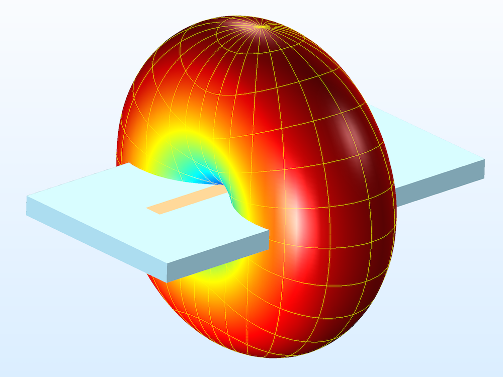
Instead, place the antenna at the edge of the circuit board and let the ground plane run close to the edge of the antenna. While a monopole antenna is different, in a dipole antenna, for example, the radiation pattern will have a zero intensity line that runs parallel to the length of the antenna (see below). The emitted radiation pattern will be orthogonal to the ground plane, and emission at wider angles will not be blocked by the ground conductor.
Multiple Ground Planes or Ground Plane Regions?
This question arises in mixed-signal systems, where digital and analog sections are placed together on the same board. Proper grounding techniques in mixed-signal systems should aim to separate digital signals from analog signals so that the components do not interfere with each other. The typical strategy is to partition the PCB ground plane into digital and analog sections, meaning to physically split the ground plane into two sections.
The idea is to prevent digital signals from interfering with analog signals. However, there are multiple reasons the ground plane should not be physically split into different sections:
- Difficulty defining clear return paths, which creates inconsistent impedance
- EMI from long return paths with large loop inductance
- Inconsistent reference potential, which creates unintended level shifts
If you do need to use multiple ground planes regions to ensure isolation, you can tie the regions together with capacitors to ensure consistent reference potential throughout the system. However, for high speed/high frequency boards, it is highly recommended to use a continuous ground plane with no splits in each ground layer. This eliminates the possibility of routing over splits or creating wide return paths with high loop inductance.
Since proper grounding is paramount to ensuring reliability, you need a PCB design software package that gives you the best design and analysis tools. PCB ground plane design is easy with the advanced CAD tools in Altium Designer®. When you’ve finished your design, and you want to release files to your manufacturer, the Altium 365™ platform makes it easy to collaborate and share your projects.
We have only scratched the surface of what’s possible with Altium Designer on Altium 365. Start your free trial of Altium Designer + Altium 365 today.

About Author
Related Resources


Related Technical Documentation


Take advantage of the world's
most trusted PCB design system.
One interface. One data
model. Endless possibilities.
Effortlessly collaborate with
mechanical designers.
The world's most trusted
PCB design platform
Best in class interactive
routing
View License Options
Thank you, you are now subscribed to updates.