How Antipads Affect Signal Integrity in Your Multilayer PCB

Antipads around through-hole vias are a point of contention in modern PCBs, and the debate around the use of these elements in a multilayer PCB is framed as a binary choice. With today’s modern PCBs, it pays to understand the effects of antipads on signal integrity, and specifically on via impedance in a PCB. In this article, we'll look closely at the effects of antipad sizing on via impedance and wave propagation because this metric is the basis for other signal integrity metrics.
How to Model Via Antipads and Signal Integrity
If you’re routing through a solid plane, the design question is how large should the antipad extend past the via pad and if any internal nonfunctional pads are kept in the design. If you look at some component application notes, they will recommend placing antipads on landing pads without explanation. In addition, different notes will tell you precisely the via antipad diameter you should use, but it is easy to take this out of context. Let’s look closely at these two situations and how the structure of a via/pad + antipad can lead to signal integrity problems.
Antipads on vias are precisely sized to hit a target impedance at high frequencies. For Dk = 3 to about Dk = 4, the frequency range where controlled impedance will be needed is slightly above about 3-5 GHz (see the model below). A via antipad can also be applied automatically by your CAD tools based on your clearance rules anytime you use a plated-through hole to transition through a solid plane. The clearance will be applied whether you keep the NFPs on your via or remove them. You could also apply a polygon cutout if the via is passing through a layer with copper pour; this would give you some flexibility to target specific vias with precisely-sized antipads.

A Low Frequency Model (up to 3-5 GHz for Dk = 3 to 4)
At low frequencies, there is a simple model that can be used to approximate via behavior. The point in applying a specific antipad is so that the via impedance can hit a specific target. This is done by balancing the standard reactive parasitics in a via structure:
- Inductance. A via taken in isolation is basically an inductor, and the inductance of the via depends on the via aspect ratio.
- Capacitance. The presence of the plane around creates some parasitic capacitance around the via wall, and there will be capacitance between the via pads and ground.
Each pad at the end of the via and the intervening plane creates two capacitances in parallel. When combined with an inductor, we have a standard pi model describing a via and their antipad, as shown below. Note that the capacitance equation shown below is only an approximation as it does not consider fringing fields. The via inductance equation is also an approximation.
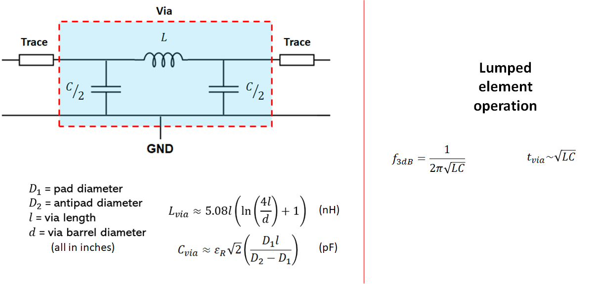
We can extract a coupld of conceptual results here. First, just like any pi circuit, the CLC pi model is basically a low-pass filter with the 3 dB cutoff frequency defined above. Suppose you want to extend the bandwidth of your via + antipad arrangement. In that case, you’ll need to reduce the aspect ratio (shorter via or wider barrel diameter), or decrease the pad-plane-pad capacitance (larger antipad). Second, there is a danger the 3 dB frequency would decrease and limit the bandwidth when the aspect ratio becomes quite large.
Unfortunately, this model will be inaccurate at frequencies above about 3-5 GHz. Why can we not use this for via impedance calculations? There are a few reasons:
- It is only accurate in ranges where the via impedance is not needed
- It tends to grossly overestimate the via propagation delay
- It does not contain frequency-dependence in impedance, which will always be observed above 3-5 GHz
- It cannot consider stitching vias and their effects on impedance for single-ended lines
- It can't be used with differential pairs, which are dominantly used with impedance-controlled high-speed signals
Once you get to the mmWave regime, you’ll have other signal integrity challenges involving routing through vias. Additional parasitics become dominant at these frequencies and contribute to overall insertion loss along an interconnect.
Example Dk-effective Calculation
Just as an example, we can use an example antipad size calculation to determine the time required for a signal to travel along a via. The travel time can then be compared with the travel for the same signal in vacuum to determine an effective dielectric constant along the length of the via.
Let's suppose we have a via passing through a 1.57 mm thick PCB with 10 mil barrel diameter, 20 mil landing pad, and 25 mil antipad. If we calculate the propagation time using the above model with Dk = 4, we get about 43 ps transit time across this via, although the real value ends up being about 20 ps with no stitching vias. That gives a Dk-effective value of about 14. That means a single via creates a lot of excess propagation delay for signals traveling along the via; if we just use the Dk = 4 value to calculate the propagation delay through the via, we would calculate about 10 ps propagation delay. That's a significant difference if we need delay-matched signals (in high-speed design) or phase-matched signals (in RF design).
Antipad Manufacturability
The size of an antipad will also affect manufacturability. The manufacturability issue here concernse drilling a through-hole via through a plane, which will be impacted by drill wander. During fabrication, any wander in the drill hit can cause the hole to be placed in the wrong location and would expose some of the plane's copper through the hole wall. During plating, this would create a short into the plane layer.
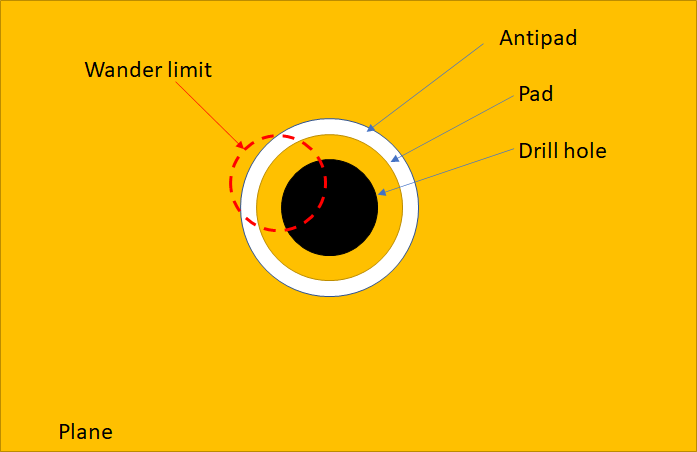
To prevent this problem, the antipad needs to be large enough so that any wander in the drill hit does not pierce the plane layer. At minimum, an appropriate approach is to make the antipad at least as large as the pads on each end of the via. However, for Class II products, any breakout in the annualr ring would definitely hit the plane layer, even if accounting for layer-to-layer misregistration (usually about 1 mil).
On this point, a good strategy is to ask your manufacturer what they recommend. One rule of thumb is to size the antipad diameter so that it is 20 mil larger than the drill diameter, or 12 mil larger than the pad size required for IPC-6012 Class II compliance. This would give you plenty of room for Class II or Class III products. This is just a recommendation; you could opt for a smaller expansion value as long as there are no non-functional pads on the internal layers, although compliance may be an issue if manufacturing tolerances are too loose.
Above the 3-5 GHz Limit
Impedance is Controlled With an Antipad, NFPs, and Stitching Vias
If you viewed the via impedance calculator article linked above, then you likely noticed that stitching vias are needed when a specific via impedance needs to be targeted. Adding stitching vias adds distributed capacitance in parallel to the via transition; this can convert the via impedance from inductive to capacitive just as the frequency of operation exceeds about 5 GHz. In most digital protocols (below 10 Gbps SerDes) and in single-ended RF interconnects, only a small number of stitching vias might be needed. In well above 5 GHz signals or bandwidths, stitching vias will be required to set the impedance to a target value.
Stitching vias are simple: they are arranged around the via along the edge of the antipad. To properly set the via impedance to be flat out to high frequencies, it is recommended to remove the NFPs and to place stitching vias around the via structure. An example structure that extends the via structure impedance beyond 5 GHz is shown below:

If the stitching vias are brought too close to the signal via, then the via impedance will change from inductive to capacitive above the ~5 GHz limit. This is because via structures are very sensitive to capacitive loading along the via wall, particularly for through-hole vias. Setting the via and antipad to just the right diameter can help set the via impedance to an ideal system impedance value (usually 50 Ohms) over a broad bandwidth, including for through-hole vias.
What About Differential Pairs?
For differential pairs, there is a bit of a different consideration as we need to examine the effect on the via structure's odd-mode impedance. In other words, we have to analyze a pair of vias that are driven differentially, not a pair of individual vias. Unfortunately, the simple low-frequency impedance model outlined above is also not useful for differential pairs and there is no analytical model for modeling differential vias as transmission lines. The typical strategy is to maintain no less than the same spacing used while routing when placing the differential vias. However, the pad sizes may limit the distance you can set between the differential vias and their landing pads. Therefore, a field solver is the best tool for accurately determining placement and routing through differential vias in a high-speed PCB.
Antipad Sizes for Backdrilling
In both single-ended and differential cases, you may need to determine backdrilling requirements, which will also depend on the antipad size. The drill bits used in controlled-depth drilling can be larger than the typical via diameter; just to be safe it is best to size the antipad such that it is larger than the drill bit. To learn more about this, take a look at the following video on backdrilling to see how antipads on a pair of differential vias affects via propagation delay. As you'll see in the video, the antipad helps determine the lowest order resonance frequency in the via stub, which will determine when backdrilling is needed.
Summary
In summary, if you want to control via bandwidth and parasitics, you have a few levers you can pull. Antipads on vias give you a simple way to tune the parasitic capacitance to match the inductance for a given via aspect ratio. The dielectric constant (Dk value only) can also be used as a tool for controlling via capacitance. Finally, stitching vias are needed to set the via transition to the required impedance above approximately 5 GHz.
Regarding antipads on landing pads, you’ll create a small impedance discontinuity, which can create some small insertion loss and return loss at the pad. In high speed channels where bandwidths can extend up to 100 GHz and beyond, every last bit of insertion loss you can avoid is critical. My view is to play it safe and not use any antipads on landing pads unless you absolutely need to do this to set a landing pad’s impedance to some specific value, thereby reducing return loss.
Whenever you need to design an antipad and place stitching vias in your PCB, you can use the complete set of rules-driven design tools in Altium Designer®. When you need to share your work with your collaborators, you can use the Altium 365® platform to share and manage your design data.
We have only scratched the surface of what’s possible with Altium Designer on Altium 365. Start your free trial of Altium Designer + Altium 365 today.

About Author
Related Resources


Related Technical Documentation


Table of Contents
- How to Model Via Antipads and Signal Integrity
- A Low Frequency Model (up to 3-5 GHz for Dk = 3 to 4)
- Example Dk-effective Calculation
- Antipad Manufacturability
- Above the 3-5 GHz Limit
- Impedance is Controlled With an Antipad, NFPs, and Stitching Vias
- What About Differential Pairs
- Antipad Sizes for Backdrilling
- Summary
Take advantage of the world's
most trusted PCB design system.
One interface. One data
model. Endless possibilities.
Effortlessly collaborate with
mechanical designers.
The world's most trusted
PCB design platform
Best in class interactive
routing
View License Options
Thank you, you are now subscribed to updates.