How to Properly Ground ADCs

Table of Contents
ADCs are fickle components that become more difficult to work with as sample rates and resolution values increase. The resolution of an ADC and its sample rate create challenges in accurate signal reconstruction, but there is one area where ADC performance is greatly impacted: the definition of ground in a PCB layout.
The way ADCs pinouts are written and the way in which some older application notes describe ADC usage creates the chance of incorrect layout and routing that then couples noise to the ADC input. The result is then incorrect signal reconstruction due to psuedorandom fluctuations in the input signal. Strong EMI can also result when the PCB layout does not allow for correct grounding of ADCs due to the stackup, physical separation of grounds, or both.
In this article, I’ll give some context to ADC pins and what they mean in terms of grounding. The EMC experts in this area will agree: the best approach in most mixed-signal systems and with most ADCs is to use a uniform ground plane, not physically separated grounds.
Bad Pin Names Lead to Bad ADC Grounding
To see how we get to a state where so many bad grounding guidelines are implemented for ADCs, it helps to look at a typical pinout for an ADC. If you’re a new designer and you’ve never read through a datasheet for an ADC, you might be surprised to find contradicting guidelines from different semiconductor vendors.
To see an example, take a look at the ADS1274/1278 from Texas Instruments. In the pinout for this part, we have two separate pins on opposite sides of the component, labeled AGND and DGND:
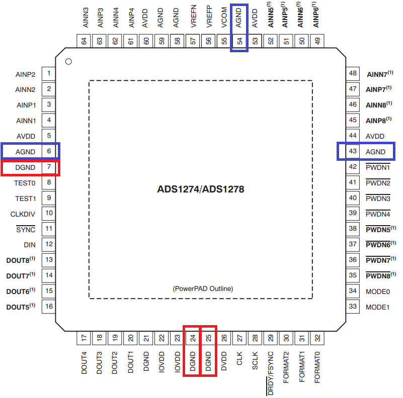
The presence of multiple GND pins, with two different names, referencing two different types of signals (analog and digital) leads to confusion that the ADC should be wired up with distinct ground potentials that must be disconnected. The other guideline you will sometimes see is to only connect them at a single point.
If you look below this figure on page 6 in the datasheet, you will see the following pin description for AGND:
AGND: connect to DGND using a single plane
Later in the datasheet, TI provides an application example with the two grounds directly connected. No net tie, no single-point grounding, just a single uniform plane for grounding the ADC.
What can create more confusion for the novice designer is the fact that other ADCs will only use a single ground pin. Another example from Texas Instruments is the ADS7138. This is a smaller ADC and it only has a single pin for GND. The pinout is shown below:

If you walk into this component with the idea that analog and digital grounds should be totally separate, then you might be surprised to find this guideline from page 4 of the datasheet:
GND: Ground for the power supply; all analog and digital signals are referred to this pin voltage
When you see the statement "referred to this pin voltage", they are telling you that the analog supply and the digital supply use this same point as their measurement reference.
Other semiconductor vendors do not always give the same correct advice. Instead, they will recommend one of two possible directions for a design:
- Tie the AGND pin and DGND pin together only at one point
- Use different AGND and DGND nets that are not connected anywhere
#2 is basically a moot point; unless you’re using an isolated ADC (see below), then there is an internal connection between these pins anyways; you will never actually separate the ground regions due to this connection in the interior of the ADC.
#1 can be okay, because at least it sets a uniform ground potential, but it is commonly implemented incorrectly. In this case, you would never be able to route over the gap between the two plane regions, so it limits your layout and routing freedom. #2 is basically the same as #1 and is a bad path forward for the same reason, except in a specific instance requiring isolation between the analog or and digital sections (see below).
Floorplanning On a Thin Dielectric Prevents Noise Coupling
For interface boards that happen to operate with a digital section and that need uniform ground, I recommend starting with a 4-layer stackup with thin outer dielectrics and ground planes on L2/L3. This gives you strong coupling for return paths for digital signals in the adjacent ground plane, and this will help prevent switching noise from coupling back into the analog side of the design.
You then don’t have the problem of using physically separated ground planes to try and prevent noise from coupling into the analog feedline on your ADC. Instead, focus on placement of components as this will help prevent noise coupling between different circuits. This is where the example pinout on the ADS1274/1278 shown above becomes; they essentially have located the pins in different areas of the component, so it is easy to implement some best practices for routing into the analog and digital interfaces.

By routing away from the component in opposite directions, you’re putting plenty of space between the digital and analog board sections. This is the best way to prevent mixed-signal crosstalk.
Now let’s look at the ADS7138 (see below). This component has an I2C interface, and notice that the data pin (SDA) runs right next to one of the analog inputs. To ensure minimal possible coupling with this component, I would route the two signals into the board in opposite diagonal directions. I would also use up all the other analog inputs before using the input that is next to the SDA pin.

Don’t Connect Power Rails With a Ferrite and Disconnect the Grounds
Another bad grounding recommendation is sometimes presented alongside power supply connections between the analog and digital power input pins. An example with the MAX11900 from Maxim Integrated is shown below.

This is probably the worst ADC-related power and grounding recommendation I have seen, and yet there are certain semiconductor vendors that have 15-year-old application notes with this advice on their websites. In fact, I have seen one company recommend doing the incorrect type of recommendation shown above, and then in the datasheet for the same component they recommend the correct connections with no ferrite and a single ground plane.
The idea in this type of recommendation is to isolate the analog rail (assumes a separate pin for the reference) from the digital rail. The idea is to confine any noise on the digital rail (which could include many different components) from the analog rail should ripple be created on the digital rail from a fast switching interface (like SPI).
You will see the same type of recommendation to isolate an analog rail on a large IC (such as a PLL reference pin on an FPGA or processor) from a digital rail with the same voltage. For something like a PLL that needs to switch at high speeds, this is something I would recommend simulating to really get a sense of the noise coupled to the analog pin within the expected noise bandwidth.
- If you want to have an isolated analog side with an isolated ADC (see below), then just make the analog rail physically separate. You can’t get much higher impedance up to many GHz frequencies than if you physically separate the two circuits!
- If you need the level of precision implied in this recommendation, you should use a charge compensation circuit on the ADC signal inputs and a dedicated precision reference/supply with its own low-pass filter.
|
|
|
|
|
|
|
|
|
|
|
|
The”less bad” and “better” recommendations are the same strategies you would use in a large processor that has an analog supply input for its PLL rails. I have seen an older presentation that suggests you should keep the ferrite, and yet we have another article on this blog showing contradictory evidence. The “better” recommendation could be used with ratiometric referencing, where the digital section is stepped down to set the analog reference value.
ADCs in Isolated Systems?
In this type of system, the entire point is to totally isolate most of the analog signal path from everything else in the system by using physically separate planes and separate power supplies w/precision referencing. However, this is challenging because you are essentially trying to couple your analog input across the isolation gap and into the analog interface, and this is only operating at low levels that make coupling difficult.
This is where you have two options:
- Use an isolated ADC that totally decouples the analog side from the digital side, and do not bridge any of the ground pins
- Use an optocoupler or transformer to bring the sampled signal across the isolation gap
A version of this is done in the transformer block and termination circuit in Ethernet; take a look at the circuit diagram in this article and see if you can spot the isolated region I’m referencing.
There is one instance where I designed a small mixed-signal board with an ADC: very low-SNR voltage measurements at nanoampere current levels running at low frequencies. Low-level noise was very problematic in this system, and the fact that we had separate equipment for source, measure, and acquisition meant that there were problems with ground loops. We amplified the signal before sampling so that the signal took up most of the dynamic range in the device, and the output serial data was given to a DAQ card for collection on a computer.
When you need to place an ADC and provide a grounding strategy for your mixed-signal PCB, use the complete set of PCB design tools in Altium Designer®. When you’ve finished your design, and you want to release files to your manufacturer, the Altium 365™ platform makes it easy to collaborate and share your projects.
We have only scratched the surface of what’s possible with Altium Designer on Altium 365. Start your free trial of Altium Designer + Altium 365 today.

About Author
Related Resources


Related Technical Documentation


Take advantage of the world's
most trusted PCB design system.
One interface. One data
model. Endless possibilities.
Effortlessly collaborate with
mechanical designers.
The world's most trusted
PCB design platform
Best in class interactive
routing
View License Options
Thank you, you are now subscribed to updates.