Huge VU-meter with RGB LEDs Project

Table of Contents
Altium Concord Pro™ as a standalone product and brand name has been discontinued and the capabilities are now available as part of our Altium enterprise solutions. Learn more here.
Introduction
Welcome! This laboratory journal will guide you through the steps to develop a successful product that value-conscious customers are sure to love. We’ll take a peek together behind the scenes of the development process. If you’re one of my customers, please look away now!
Let’s get started by airing the dirty laundry!
In my role as an engineer, my primary responsibility is to develop scientific equipment that is used to teach physics, material science and electronic engineering. Most of our clients are universities that subscribe to teaching with a ‘hands-on’ approach, rather than the typical, ‘I speak, you listen’ approach often found in lectures. The difference with teaching ‘hands-on’ is that your students are less likely to forget everything they have learned once exams are over. Let’s be honest, we’ve all been there at some time or another.
The product I will be working on in this article will be a display part of my company’s line of Microwave Optics instruments. This line of products outputs a square wave on a 3.5mm audio jack connector, meant to be interfaced with audio devices such as speakers.
Today’s goal is taking this output and doing something with it. Feeding it to the cat, using it as Christmas decoration, adding hemp powder and selling it as a smoothie, anything but letting our customers figure it out by themselves.
That would be too educational.
The Problem to Solve and the State of the Art
Our optical platform is composed of a transmitter, a receiver, and a bunch of mechanical and optical components you can place between the two, such as reflectors, lenses, and polarising filters.
The receiver outputs an audio signal proportional to the received RF power, usually a 650Hz square wave of variable amplitude.

The whole point of this product family is to move the receiver and transmitter around, insert various accessories, and see how the user action’s influence the output.
Great, now that we’ve settled that, here’s the issue: It’s not good enough.
Most of our customers connect to our product in one of the following ways:
- Speaker: easy to use, but no quantitative measure
- Sound card: quantitative measure is possible, but difficult to set up. In addition, the most widely available softwares are only supported on Windows, and the measurements tend to be very unreliable due to the automatic gain compensation present in many sound cards.
- Oscilloscope: expensive, suitable for universities but too complicated for high schools. When using measurements, the numbers are tiny and impossible to ready. Some oscilloscopes can be connected to a projector through a video output, but they’re not that common.
- Analog multimeters: They naturally filter out the noise and are easy to read, but would still require AC-to-DC circuitry as AC voltmeters are quite rare. Good-quality analogue multimeters can be expensive.
All of these solutions have pros and cons. None of them satisfies all requirements set by our customer at the same time:
- Affordable (schools don’t have that much money laying around)
- Visible for afar
- Quantitative (you can take the measurement and write it as a number)
- Responsive and intuitive to use
- Quick to set up
- No computer required
The Solution: A Giant VU-meter Stick
Vu-meters are devices used to display the volume of audio signals.
Audio voltage levels are legacy holdovers from the early telephone days with almost-archaic measurement systems. The nominal level is based on sound pressure, and for most consumer equipment, the maximum amplitude of the signal is around 2Vpp.
|
Use |
Nominal level |
Nominal level, VRMS |
Peak amplitude, VPK |
Peak-to-peak amplitude, VPP |
|
Professional audio |
+4 dBu |
1.228 |
1.736 |
3.472 |
|
Consumer audio |
−10 dBV |
0.316 |
0.447 |
0.894 |
Digital LED Vu-meters as a generic product concept satisfy all requirements, but no VU-meter is available commercially with a linear response. They’re meant to measure sound pressure in decibels. As human sound pressure perception behaves in a sort-of logarithmic way, their scale is logarithmic.
Additionally, VU-meters usually operate in a single fixed range, but for our purposes, the display should have controls to accommodate different input levels.
Let’s create a “VU”-meter that fits our needs! In the process, let’s make it as big as it’s reasonable. As always, size is mostly about putting our competitors and their puny little analogue gauges to shame.
General Requirements
Scale and Offset Control
After several trials and tribulations, we learned that when measuring the small differences in signal strength between the two positions of the receiver, the user would do well to add a negative offset in order for multiple displays to show the difference between the two signals. The scale needs to be selected by the user as well, to account for different attenuation levels between receiver and transmitter.
Perhaps unsurprisingly, this is very much like the controls on an oscilloscope: scale and offset.
LEDs
The display should be visible in a well-lit room (my Swedish customers take getting their daily dose of sunlight very seriously) but not bright enough to be annoying.
The general rule of thumb to choose LEDs based on their luminous intensity is:
- 50mcd for a cheap indicator LED
- 100mcd for a high-quality, bright, indicator LED
- 300mcd and over for interior decoration (for the red element of an RGB LED only)
Full Specifications
Ideally, we would need a VU-meter-like device with the following specifications:
- Easy to see from a distance
- Bright enough to be visible in a well-lit room (100mcd)
- Not too bright to impair vision (less than 50% power standard 5050 RGB LED)
- 25 to 50 LEDs
- Each LEDs individually numbered
- Linear response
- Analog offset and scale control, similar to oscilloscopes
- Cheap and sturdy
The basis of any circuit design is some napkin system engineering; let’s break the problem down into manageable components.

Processing Block
So, now we have an oddly shaped square wave. We want to measure Vmax-Vmin, ignoring as much as possible of the noise and the peaks, especially the rather nasty overshoots that can happen when the receiver is approaching saturation.
The square wave currently looks like this in the best-case scenario:
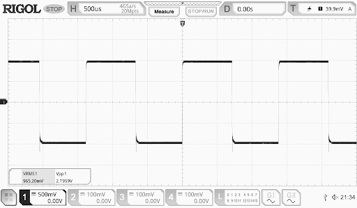
It all sounds so easy, but the devil is in the details.
We can make the square wave prettier and attenuate some of the noise through a low pass filter. The overshoots and undershoots at the transition regions of the square wave are, however, quite hard to deal with.

Why do these overshoots happen? There are three main reasons:
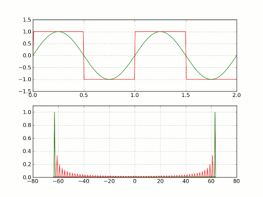
The first is the Gibbs Phenomenon. In the frequency domain, a square wave is composed of an infinite number of equally frequency-spaced harmonics. When we filter a perfect square wave with a low-pass filter, either intentionally or simply through the physical limitations of our hardware (for example, parasitic capacitance and resistance), we are attenuating the high-order harmonics. When a square wave is approximated by a finite instead of an infinite number of harmonics, it presents a natural “ringing” phenomenon, with an overshoot and undershoots near the rising and leading edges. This phenomenon is intrinsic in the math and physics of signal, and there is no escaping it.
The second phenomenon that may occur is ringing due to the parasitic components of our circuits. Any parasitic capacitance and inductance can create a resonant circuit. Since the edge of the square wave is rich in high-frequency components, something will likely resonate.
The third phenomenon commonly attributed to causing these oscillations is transmission line reflection. Still, it’s just a corollary of what we discussed already and doesn’t apply at our frequencies of interest (unless you use viciously long cables).
Things get a little bit more complicated when we take a look at the worst-case scenario when the signal can be down in the tens of mV, and the signal presents a low SNR (Signal to Noise Ratio).

So, how can we convert this square wave to a single value we can display?
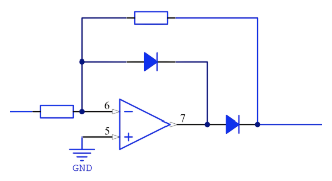
Technique 1: Analog Rectification and Filtering
The most straightforward approach to go from AC to DC is rectification.
For small signals, diodes alone won’t work, as the forward bias voltage of a diode (round 0.7v) is almost as high as the signal we want to rectify in the best-case scenario, let alone when we’re talking about 40mVpp.
A precision rectifier solves that problem, by using the opamp’s feedback to bypass the forward bias altogether.
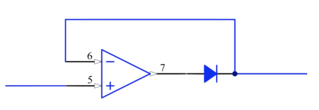
Books will tell you that you can implement this circuit in a single-diode or double-diode configuration for a half-waveform rectifier and full-waveform rectifier respectively, however, I don’t recommend even attempting the single-diode circuit. The op-amp will be in saturation the majority of the time, leaving you with performance orders of magnitude worse than what you might expect from the datasheet.
Go instead with a double diode configuration.
We can easily simulate the effect of a rectifier by using the ABS function on the math channel of a digital oscilloscope.

As you can see, the output of (just) a rectifier can be a messy signal. Any DC bias before the rectification stage must be eliminated entirely; otherwise, a ripple will be present. A rectifier by itself does not attenuate the noise or get rid of the overshoots/undershoots, that instead become positive impulses in the output signal.
Technique 2: Peak Detection
The measured values displayed on the LED must be stable and docile; we can’t allow the LEDs to follow peaks, overshoots, and other spurious signals. If we did so, human persistence of vision would kick in, and multiple LEDs would appear lit at the same time.
We need some way of slowing the signal down, and a peak detector following the precision rectifier discussed earlier might do the trick.

In a peak detector, the diode is forward biased when charging the capacitor, and reverse-biased when discharging it. A high-value resistor can be placed to discharge the capacitor at a known rate.
The peak-detector smooths out the incoming signal to almost DC levels and slows down the rate of change to a level the user’s eye can follow.
The disadvantage? The circuit would trigger on overshoots and undershoots instead of the stable part of the waveform, which is precisely what we don’t want.
We could mitigate this by placing a resistor between the op-amp and the capacitor so that the rate of charging is limited during fast events.

Technique 3: RMS to DC Converter
A more sophisticated approach is to use an RMS to DC converter, a family of integrated circuits specialised in converting any waveform to DC.
When you see a multimeter with a tru-RMS feature, there’s one of those inside it.

Unfortunately, RMS to DC converters can be quite pricey. An AD8436, one of the most popular models, will set you back between $3 ad and $5 depending on the supplier and quantity. My wallet is screaming in pain already!
RMS to DC converts can be used to replace a precision rectifier, but will still require a fair amount of filtering before and after.
In this case, though, it doesn’t make much sense: we know in advance the signal is a square wave, so what’s the point in using an IC that exists primarily to adjust for the difference between differently shaped signals?
We also want to ignore the peaks, while RMS to DC converters will include them in their calculations.
Technique 4: Digital Processing
Digital Processing. The last frontier.
Our input is an audio signal, and audio signal processing is one of the most well-studied (and well-documented) fields of electronics, with countless application notes, example circuits and ready-made ICs available.
Our output will be a strip of LEDs. LEDs are almost always controlled digitally, either ON-or-OFF or with PWM (Pulse Width Modulation). The sooner we go-digital, the more analogue components we can replace with a single MCU, the fewer lines our BOM will have and thus the cheaper the product will be.
Another excellent reason to go full-digital is intellectual property protection. One of my (former) customers recently decided they’d copy my product and make it themselves. The product is now a world-wide best-seller, and I’m not seeing any of that sweet, sweet money.
I’d rather not repeat that experience twice. For that reason, I’m inclined to use an MCU (Marvel Cinematic Universe?), encode some bad poetry about my long lost first romance inside the firmware, and sue for copyright infringement whoever tries to take advantage of my work.
The last reason why going digital can be advantageous is that we can use cross-domain techniques, working in both the frequency domain through analogue and digital filters and the time domain through more straightforward code. We can even take it a step further, ditch the electronics altogether and approach the problem as a statistician would.
Tasks such as converting a noisy AC signal into a single value are much easier when you can take thousands of samples and calculate a moving average.
And honestly, microcontrollers are kinda fun, and I’m tired of spending my time tweaking the resistor values in Chebyshev filters.
The previous are all, in my opinions, excellent reasons to go digital.
Circuit Design
MCU Selection
We need to select an MCU with: - 4 analogue input, at least 12 bit, ideally 16 bit - fast ADC so we can average many readings and reduce the noise (100ksamples/second) - one digital input (to sense when the input jack is present). This is not strictly necessary, but it can be used to improve the user experience, for example, by shutting off all LEDs when no jack is present to avoid displaying noise. - Price under 2USD in quantity - Widespread adoption and excellent development tools
I cross-referenced a few MCUs between the manufacturer data and various suppliers using Octopart and settled for a STM32G031K6T6 Arm Cortex M0+ manufactured by ST. Here are some of the reasons: - Darn cheap, at less than 1USD/piece - Latest generation with 10years guaranteed availability - 12 bit ADC with 16-bit hardware oversampling - available high-performance open-source libraries to manage the WS2815 LEDs - Really good IDE
ST IDE’s used to leave much to be desired, but since the acquisition of Atollic, they’re offering the famous Atollic Truestudio rebranded as STM32CubeIDE.
ADC Calculations
Let’s do some (very) rough math to make sure our ADC performance is enough.
Our output display will have around 25 LEDs (the number will be finalised during PCB design). Let’s round up to the nearest power of two, so we can make some back-of-the-envelope calculation without getting headaches to 32 LEDs, or 2^5. Our ADC has 12 bit, and we can oversample up to 16 bits in hardware.
To make sure we can display a full-scale signal of around 40mVpp we are going to need a resolution of 1.25mV with 32 LEDs, and at least log_2(3.3V/1.25millivolts)=11.37 bits of resolution.
We have a 12 bit ADC, so everything is fine and dandy, right?
In reality, the 12-bit resolution of our ADC is a theoretical value influenced by many factors, and we should be highly sceptical of it. What we should look at is ENOB, or Effective Number Of Bits, 10.2 for the STM32G031G8 as indicated in page 81 of the datasheet.
Remember: resolution is for the fools, ENOB is for the wise.
Good thing I chose a microcontroller with hardware oversampling so that we can reach an (extremely) theoretical resolution of 16bits.
Hardware Oversampling
Our ability to use the hardware oversampling to 16bit of resolution of the ADC depends on a series of factors. Oversampling is a technique where a signal is sampled at a frequency significantly higher than the Nyquist rate and then compressed, usually (but not always!) by averaging it out.
For effective oversampling, three criteria must be respected. First, the predominant noise source should be white noise, or at least look like it over the frequency band of interest. White noise has a uniform spectral density, a fancy way of saying it’s flat if you look at it on a spectrum analyser. I don’t have a spectrum analyser, so I’ve tested it with my oscilloscope’s FFT (Fast Fourier Transform) on the stable part of the waveform, and it looks pretty flat.

Second, there must be enough noise to shuffle the samples around, at least 1LSB. Third, and this can get complicated, the input signal should have the same statistical probability of existing at any intermediate values between the two LSB. This last point can quickly get complicated if approached theoretically, while it’s relatively easy to deal with experimentally. Let’s skip over it for now and hope for the best.
There are so many factors that influence the ADC’s sufficient resolution, including many we have not yet considered (such as power supply noise). I am not 100% sure we can have enough significant bits at the necessary sampling frequency. For this reason, I think it would be best to include some optional amplification.
Ancillary Components
The STM32G0 series of MCUs have almost no external components. I have added the necessary bypass capacitors, two potentiometers to set the scale and offset, and that’s about it. Since there are no external clock sources, we’ll use the internal RC and PLL.
I’ve added a test point on pin PF2, as it can be used as a clock-out pin to check if everything is running correctly. We don’t need a reset circuit. The MCU has full internal reset, which is an all-in-one solution.
Input Block
Our input is a square wave with the following characteristics:
- 1Vpp to 2Vpp nominal depending on the configuration
- Max 5Vpp when the devices are placed in close proximity and the receiver has saturated
- Quite noisy (see previous and following images)
- Possible DC offset of +- 300mV
- 650Hz +- 50Hz
- Square wave with considerable overshoot and undershoot
- The value to be measured is Vmax-Vmin, not Vpp (Peak to Peak)
- 3.5mm mono jack with the signal on the tip and ground on the skirt
As Einstein said, “Only two things are infinite, the universe and human stupidity, and I’m not sure about the former.”
In reality, educational equipment might be used by barely-supervised teenagers, or worse, their professors. As such, we want to make sure the inputs are adequately protected, for example, by adopting 25kV ESD discharge protection (IEC 61000-4-2 25KV).
We want to minimise possible damages to the equipment that may result from a reasonable amount of misuses. These issues could arise from school students unintentionally zapping their devices with ESD simply by wearing polyester hoodies during winter, or someone plugging the wrong connector into the wrong place.
If possible, it would be nice to have some over-voltage protection in the power supply input. Common wall-plug power supplies can be found up to 24V, and bench power supplies usually reach up to 36V.
Input Block Design
The output of the receiver is a simple voltage follower followed by a 10uF series capacitor.

The input signal enters from pin 3 of the jack connector and goes through a capacitor C11. C11 should be omitted, as the signal is already AC coupled from the output capacitor, but it’s presence enables the instrument to be compatible with a broader range of sources. If needed, C11 can be shorted by a resistor of the same case size (0805).
As we all know, two 10uF capacitors in series would halve the capacitance, and this would end up distorting our square wave further than necessary.
The capacitor would be the first component to be zapped by an ESD event. However, research has shown that capacitors over 10nF can resist 25KV Body Model ESD tests. This capacitor is 1000 times bigger, so it should be ok.
The diode D1 is a particular kind of diode called TVS (Transient Voltage Suppressor). They’re made of two Zener diodes in anti-series and are able to withstand tremendous impulse currents. During an ESD event, the diode will go into breakdown mode and clamp the voltage to about 6V, ensuring no high energy pulses can reach the delicate op-amps and microcontroller. The diode is a last measure, as the capacitor C11 should absorb most of the energy.
The op-amp circuit is a simple inverting amplifier. R10 and R11 create a voltage divider Vout=3.3/2=1.65V while C1 54 creates a low pass filter with R6//R7 with a corner frequency of f = 1/(2 x pi x R x c) = 1/(2 x 3.14 x 5 x 103 x 10 x 10 - 6) = 10.61Hz that will dramatically reduce the influence of power supply noise. Without it, our circuit would have an obscene PSRR (Power Supply Rejection Ratio) around 0dB!
Thanks to the negative feedback of the op-amp circuit, the 1.65V voltage on pin1 is maintained as a virtual ground on pin 3 as well. The total DC gain of the amplifier is unitary, with G=R6/R5=1, allowing us to measure up to a theoretical 3.3Vpp of AC signal (the operational amplifier is rail-to-rail).
C12 creates a low-pass filter that we’ll use as an anti-aliasing filter. Any digital sampling system must respect the Nyquist-Shannon theorem: to reconstruct an analogue signal through digital sampling, and it must be sampled at least two times the maximum frequency of interest. Any signal of frequency higher than half the sample rate cannot be sampled correctly, and it is labelled under-sampled.
(I took some poetic license on the theorem for the sake of clarity and context)
Flipping the equation on its belly, you get the issue of aliasing. If you have a signal with a higher frequency than half your sample rate, and try to sample it anyway, aliasing kicks in and creates weird artefacts.
To avoid that, the simplest solution is to low-pass the signal. For now, I configured the filter with a corner frequency of: f = 1/(2 x pi x R x c) = 1/(2 x 3.14 x 10 x 103 x 1 x 10- 6) =15.92kHz
The filter can be easily adjusted during testing of the ADC if needed. At the moment, I am not sure what sampling frequency I will use, so there is no point in overthinking it.
The resistors R4, R7, and R10 are not strictly necessary. Still, they are there to avoid damaging the op-amp or the microcontroller if the latter’s I/O are erroneously configured as outputs instead of analogue inputs. They will create a second low-pass filter with the internal 6pF sample capacitor of the ADC. However, this will have almost no influence on the measurements as the corner frequency is much higher than the signal we want to measure.
f = 1/2(2 x pi x R x C) = 1/(2 x 3.14 x 103 x 4 x 10-12) = 37.79MHz
The ADC will also sample the 1.65V signal so that it may be subtracted directly, significantly improving the precision with small signals.
For the optional amplification stage, I added a second inverting amplifier chained to the output of the first and connected to the same virtual ground, with a gain G=R9/R10=10k/1k=10, that will bring our theoretical single-led resolution (that truly should be called LSD!, Least Significant LED) to 0.161mV, or a 5.15mV full-scale at 32 LEDs.
If the second amplifier is not sufficient, we can increase its gain to 100.
Display Block
I know I want a LED bar already, but what kind?
Let’s explore some options.
Individual LEDs Mounted on a PCB
A simple option is using individual LEDs, that can be controlled using an LED driver.
My go-to signal LED is a 5mm red model with MPN 333-2SURD/S530-A3 manufactured by Everlight Elec, with a nominal forward bias current of 20mA, a forward voltage drop of 2.0V and about 100mcd of luminosity.
An LED driver IC, such as STP16CP05 can integrate all the digital and analogue circuitry necessary to pilot a virtually unlimited number of LEDs. Many knock-offs exist and can help reduce the cost further if needed.
Digital “Pixel” LED Strips and LEDs
Commercial interior designers love digitally addressable light strips, especially China and South Korea. You can hardly walk thirty steps in Shanghai without a full indoor-rainbow screaming at you from a shop window.
The *NeoPixel is one of Adafruit’s best selling products, and it’s just their brand-name for the daily variety of WS2812B, SK6812 or APA102-based digitally-addressable LEDs.
Digitally addressable LED strips work as a FIFO serial-to-parallel converter that moves information about the amount of brightness from one end of the strips to the other, shifting it by one LED at a time.
While in theory, the nature of the unidirectional flow would conflict with the way a VU-meter is meant to operate, in practice we should be able to refresh the whole strip of LEDs quick enough for the persistence of vision not to kick in.
Circuit Design
Our target luminosity for the LEDs is 100mcd. The WS2812A has a maximum consumption of 20mA for each colour channel, with the Red channel producing 550 to 700mcd. Light intensity decreases linearly with the current in most LEDs, and for sure it decreases linearly when PWM is used, so we can expect to power them at 1/5 their nominal power, or 4mA each.
WS2812C would be even better for this application, as they have full-power of just 5mA and are more affordable.
25 WS2812C LEDs would consume 5mA*25=125mA and be powered at 5V.
We need to find a way to power this instrument without it catching fire, the user getting burned, and ideally, without using a second power supply for the rest of the apparatus that will confuse the user and will eventually lead to someone swapping power supplies.
All of our products are powered by a 12V switching power supply able to supply up to 1A. However, 12V is very far from the LED forward voltage, typically between 1.8V for red LEDs and 3.6V for white blue/white LEDs, and still very far from the 5V supply of the WS2812C LEDs. With our nominal current consumption of 125mA, and Vdo=12−5=7V, we would have 875mW of wasted power, almost a whole Watt. We’re already in the territory where we would have to use reasonably bulky linear regulators and consequentially find a way to dissipate the resulting heat into the case. DC-DC converters would be more efficient, but also more expensive and always imply a greater risk of not passing EMC certifications.
Luckily for us, WorldSemi has introduced a new WS2815 LED with 12V power supply. It costs about 30% more, but it saves a lot of trouble.
We will still need the 3.3V supply for our microcontroller, and 5V supply for the TTL communication required by the LED through a voltage translator. I’ve selected 74LVC1T45W6-7 from diodes, as it’s among the cheapest on the market, comes in a lovely sot-26 package and is bidirectional with externally configurable direction.
There are many automatic bidirectional switches, but they’re always a source of trouble and should be used only for open-collector busses such as I2C.
Drawing with Altium Designer and A365
Enough talk, let’s lay some chips and get our hands dirty!
To get started with Altium Designer® and Altium 365™, first of all, check you’re logged-in correctly. If you are, the little cloud icon will be blue.

Create a new cloud project under File, New, Project, and make sure you have enabled Formal Version Control to take full advantage of Altium 365. It’s GIT capabilities that we have discussed in-depth in a previous article.

I like to create new schematics and PCB documents in advance, so I can save them and name them in a way that makes sense. To do that, right-click on your newly created project, and use “Add New to Project”. In this case, we want to add two SchDoc and one PcbDoc and save them with appropriate filenames using CTRL+S.
We now have an empty schematic… so, now what? Let’s start with our queen, the microcontroller. At first, I attempted to use the Manufacturer Part Search and looked up if the symbol and the footprint were available, but unfortunately, they weren’t. No worries, drawing one only takes a few minutes.
Easy peasy. File, New, Component, then select the appropriate category, in this case, Integrated Circuits.
Note: In Altium 365 categories are mapped to templates and are fully editable.
When you type the MPN (Manufacturer Part Number) in the component name field, the field is automatically populated with data from Octopart. Confirm the correct component by clicking on it, and the datasheet will be fetched automatically, together with supplier information.

To create the symbol, firstly I exported a CSV pin list from the STMCube32IDE’s configurator and copied the columns on interest (Position, Name, and Type) without the column name.
Create a new symbol with the Symbol Wizard, and press CTRL+Shift+V to activate the smart-paste feature. In the “Pin Data Smart Window”, select the right column names and confirm.

For the footprint, I was in luck. Mark Harris’ wholesome Celestial Library already contained the right QFN package from ST, so I just copy-pasted the content inside a new footprint.
Once you’re done with populating the data, including optionally component parameters, you can right-click on the component name and save to the server.

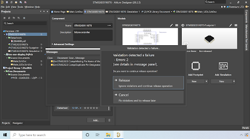
When you use Altium Designer the old fashioned way (without Concord Pro™), component data is validated when the design is compiled. With Concord Pro, the component is validated when you try to save it. In this case, I made a very dumb mistake: I placed an extra pin.
After all the mistakes were fixed, I saved the component in the server following the default revision plan.
Rinse and repeat for all components. When models are available, you will be offered the possibility of importing them automatically.

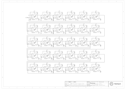
Conclusion
In the following two figures, you can see the resulting preliminary schematic we have designed. Components such as the DC connector and the op-amp were imported from an Altium DBLib as described in the article “Altium DbLibs and Electronic Components in the Cloud with Altium Designer 20.1”, while others were created with the same procedure we described. Additionally, the schematic document was styled with the free template included in the article “Perfect Styling for Your Organization with Altium 365: How to Keep Schematics Organized".
The design tools in Altium Designer contain everything you need to keep up with new technology. Talk to us today and find out how we can enhance your next PCB Design.

To design a product your customers will love, you have to delicately balance countless compromises, carefully and thoughtfully evaluating each tradeoff along the way.
Altium Concord Pro and Altium Designer can aid you at each step of the process by enriching your library with up-to-data component market data and ease of the burden of development with seamless component management and cloud project storage, with all the power of Git under the hood.
1Electrostatic Discharge Analysis of Multi Layer Ceramic Capacitors


About Author
Related Resources


Related Technical Documentation


Take advantage of the world's
most trusted PCB design system.
One interface. One data
model. Endless possibilities.
Effortlessly collaborate with
mechanical designers.
The world's most trusted
PCB design platform
Best in class interactive
routing
View License Options
Thank you, you are now subscribed to updates.