Near-field and Far-field EMI: What's Causing Noise Problems in My PCB?

If you’re an antenna designer, then you’re likely familiar with all aspects of near-field vs. far-field radiation. Given the litany of radiated EMI problems that cause noise within and outside of an electronic device, one might suddenly realize their new product is acting like a strong antenna. To understand how EMI affects your circuits, it helps to understand exactly how near-field vs. far-field radiation from your PCB affects your ability to pass EMC checks and affects your circuits.
As we will soon see, radiated EMI within a device is typically caused by near-field radiation, which can arise due to poor isolation, stackup design, grounding, or shielding. In contrast, the behavior of radiation from a device is tested in the far field in order to examine how it transmits radiation to another product, potentially inducing noise and interference in the victim device. Here’s how each type of radiation works and what distinguishes the near-field vs. far-field.
Near-field vs. Far-field Radiation and EMI
Distinguishing the two types of radiation requires comparing the distance from the source of any radiated EMI to the wavelength of the radiated signal. In the near-field regime, the distance between the source and the receiver is much less than the wavelength. In the far-field regime, the opposite is the case; the distance between the source and receiver is much longer than the wavelength of the emitted radiation. As radiation is emitted from a source, the it eventually propagates away from the sources as a plane wave, or as a spherical/ellipsoidal wave.
In EMC testing, the strength of emitted radiation is measured in the far-field regime rather than the near-field regime. Very close to or within the near-field, the radiation pattern from the source is still influenced by the geometry of the source, and the electric field may not have stabilized into a clear harmonic signal or propagating pulse envelope. As various noise sources in a PCB can radiate at a variety of frequencies, the signal being measured will be a simple superposition of the various noise signals. This produces the noise spectrum that is normally measured in EMC testing.
The two regimes are also defined in terms of the free space impedance seen by the magnetic and electric fields in a propagating signal. In the near-field, the magnetic field intensity is stronger than the electric field, thus magnetic induction will dominate noise. There is an intermediate regime, called the Fresnel regime, where the wavelength is similar to the distance from the source. Within the Fresnel regime, the magnetic field strength quickly becomes very similar to the electric field strength. In the far-field regime, the two field strengths are equal. This is summarized below.
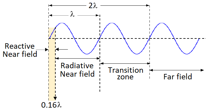
Far-field emission power is the primary quantity measured in EMC tests, although nearby devices emitting at long wavelengths (e.g., within 1 to 10 m for emission at 30 MHz) will still put EMI into the near-field regime in nearby devices. The reason for the far-field measurement is that one can use it to calculate the strength in the near-field and Fresnel zones, giving you a full view of EMI susceptibility in all important regimes.
Near-field Radiated EMI in a PCB
In a PCB, the field emitted by a radiating portion of a PCB will generally be in the near field, even with fast digital signals (e.g., with bandwidth up to 20 GHz), or it will be in the Fresnel zone in larger boards. The exception is in mmWave boards running above ~75 GHz, where the wavelength gets down to 1 mm in a substrate with Dk = 4, thus radiated EMI is in the far field. What happens in a real board in terms of crosstalk depends on whether we are looking at digital or analog signals.
Near-field EMI from Analog Signals
As near field radiation is strongly magnetic, it will primarily be received via magnetic induction. Even at high frequencies, inductively coupled near-field EMI can be received as crosstalk by closely spaced traces. At sub-GHz frequencies, strongly radiated EMI could be received anywhere in the board unless the board is very large. In essence, every circuit in your board acts like a set of coupled inductors and can receive harmonic tones at any frequency. This should illustrate the need for strong isolation between critical circuit blocks.

Near-field EMI from Digital Signals
Again, near-field radiation is always strongly magnetic, but an inductively coupled signal will only be induced in a nearby trace during a switching event. In this case, describing the behavior of these pulses in the near-field requires use of an impulse response function in free space. The signal processing community should be familiar with this idea. In essence, this will produce the classical inductively coupled crosstalk spikes (FEXT and NEXT) most designers are familiar with.
Solving these near-field radiated EMI problems is just a matter of suppressing crosstalk. Since the near-field regime is magnetically dominated, the primary design solutions are: Decrease loop inductances with smart stackup design and trace sizing; Use surface layer gridding with isolation structures to suppress radiated EMI between circuit blocks; Add an EMI filter on critical circuits where necessary/feasible.
Before implementing any of these solutions or other innovative solutions, you’ll need to identify nets that are highly susceptible to crosstalk. The signal integrity tools in Altium Designer® will take your layout data and use it to calculate crosstalk waveforms using an integrated 3D electromagnetic field solver. You won’t have to work out any complicated near-field vs. far-field EMI calculations by hand as you design your board. No other design software contains so many powerful PCB design and layout features in a single program.
Now you can download a free trial of Altium Designer and learn more about the industry’s best layout, simulation, and production planning tools. Talk to an Altium expert today to learn more.

About Author
Related Resources


Related Technical Documentation


Table of Contents
Take advantage of the world's
most trusted PCB design system.
One interface. One data
model. Endless possibilities.
Effortlessly collaborate with
mechanical designers.
The world's most trusted
PCB design platform
Best in class interactive
routing
View License Options
Thank you, you are now subscribed to updates.