PCB Layout Cleanup Before Manufacturing

Table of Contents
Once you finish your placement and routing in your PCB layout, it can be tempting to wrap up the layout and send everything in directly to manufacturing. The reality is that the board may still need some work before it is considered finished. The cleanup you perform at the final stage of PCB layout will help you catch any outstanding errors that can't be programmed into your DRC engine, and it gives you a chance to add any outstanding details to the surface layers.
This final section of our crash course in PCB manufacturing details what needs to be done to finalize a PCB layout before generating the final deliverables needed for manufacturing. The process starts with cleaning up the surface layers in your PCB layout, where silkscreen elements are cleaned and copper elements are verified for conformance to design rules. Once the PCB layout is cleaned, you generate the finalized deliverable files and prepare everything for production.
Cleaning Up Your PCB Layout
PCB layout cleanup gives you a chance to add all the required finishing touches to your CAD data. This involves making some final adjustments to the PCB layout so that the design is in compliance with DFM/DFA requirements. Some of the important points to check in your PCB layout are shown in the table below.
|
|
|
|
|
|
|
|
|
|
|
|
Many of these points can be programmed into your DRCs and will be applied automatically as you create the PCB layout. However, it is still important to check many of these points manually as the automated DRC engine in your PCB design software might not flag these points visually. Running a final manual DRC and checking visually will help you identify any of the points in this table that were missed.
Configuring Your Test Point Requirements
Defining proper test points on a board layout during your design process is critical for having your PCB tested and verified by your manufacturer before the PCBA is sent off to you. By adding proper test points on a board, you will significantly increase the likelihood of detecting any manufacturing related errors during the post-production validation process. Given that every design has its limitations and unique physical constraints, it is always recommended to consult with your manufacturer to determine the ideal placement of test points.
Before going into the specifics of test point and pad requirements, there are several general guidelines to keep in mind.
- Each node on your board should have at least one test probe point.
- It is not recommended to use component leads as test points.
- It is recommended to distribute your test points throughout your board.
Test points can simply be exposed bits of copper on the PCB, which can be as simple as placing a pad and connecting it to a net. The typical pad size in this case can be as small as 1 mm and it can brach off from a component pad, trace, or connector. Vias connected to pads or traces are also an option to select for use as testpoints in a PCB layout, just make sure they are not tented. An example is shown below.
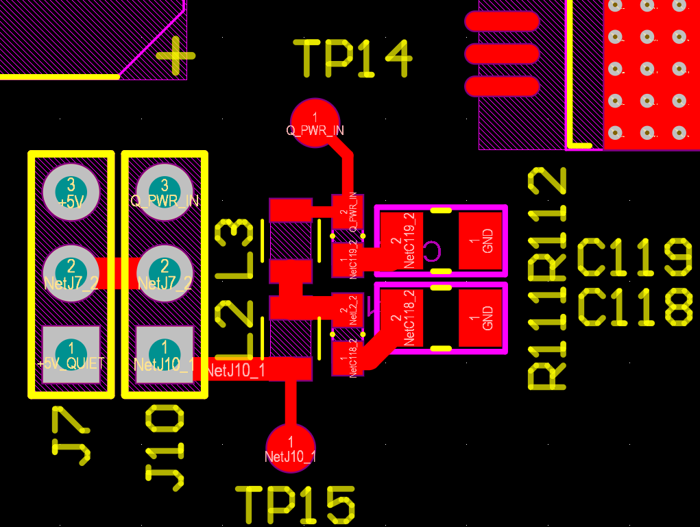
One common strategy to speed up testing during fabrication, as well as electrical testing in the PCBA, is to place the test points in a row just as you would place mounting pads for a through-hole pin header. The spacing between the test pads (center-to-center) would be maintained at 100 mils if you go this route. This allows a test fixture to easily probe all the points simultaneously.
When placing and selecting testpoints, you can define whether they should be probed during fabrication, assembly, or both. This will be done in your PCB design application, and your deliverables tools will generate a testpoint report from your layout data.
Generate Deliverables
The final deliverables package includes everything a PCB manufacturer would need to build and assemble the PCB. The final design data is seldom used by a manufacturer unless you contract them to produce deliverables on your behalf. In the vast majority of cases, you will need to produce the deliverables yourself and send these in to your manufacturer. The typical list of deliverables required for fabrication and assembly includes:
- Fabrication files (Gerber files, ODB++ files, and/or IPC-2581 files)
- NC drill files for automated drilling equipment
- A pick-and-place file for automated assembly machinery
- A wire netlist for testing (IPC-D-356A netlist format)
- A testpoint report detailing fabrication and assembly testpoints in the PCB layout
- A complete BOM with sourcing information for each component
- Fabrication and assembly drawings detailing how the board is to be manufactured
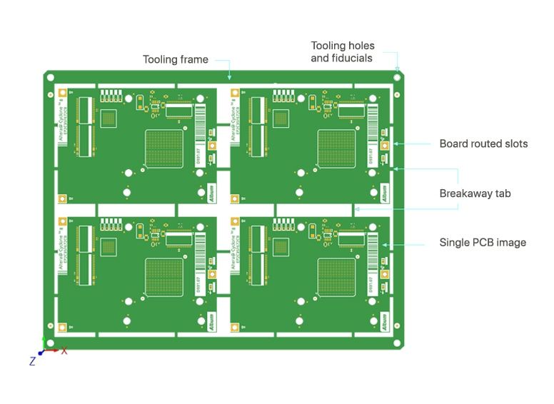
Some manufacturers might also require you to create a panel for your PCB. A panel drawing shows the arrangment of PCBs that will fabricated in a standard size panel. Once the panel is fabricated, the individual boards will be assembled in a standard soldering process.
Your PCB design software can speed up creation of these deliverables with some automated tools. Make sure you understand the complete list of deliverables your manufacturer needs as you work to clean up your PCB layout and finalize the design.
When you're ready to start your design and you want to make sure you meet every DFM requirement, use the design and layout features in Altium Designer®. Once your design is ready for a thorough design review and manufacturing, your team can share and collaborate in real time through the Altium 365™ platform. Design teams can use Altium 365 to share manufacturing data, project files, and design reviews through a secure cloud platform and in Altium Designer.
We have only scratched the surface of what’s possible with Altium Designer on Altium 365. Start your free trial of Altium Designer + Altium 365 today.

About Author
Related Resources


Related Technical Documentation


Take advantage of the world's
most trusted PCB design system.
One interface. One data
model. Endless possibilities.
Effortlessly collaborate with
mechanical designers.
The world's most trusted
PCB design platform
Best in class interactive
routing
View License Options
Thank you, you are now subscribed to updates.