PCB Layout Guidelines for Switching Power Supplies and Regulators

Table of Contents
Power supplies and regulators can come in all shapes and sizes. While they are normally discussed as different products, they are equivalent electrically, particularly switching regulators. From a high-level system perspective, the switching regulator section in a power supply and the actual regulator circuit perform the same functions within the same block diagram.
For a power supply, it’s simply a matter of scale and how the regulator integrates with other power conversion blocks in the system. The switching regulator section in a power supply, and the switching regulator circuit on a PCB, should be laid out under the same general guidelines to ensure low-noise operation.
In the forthcoming sections, I want to briefly focus on how power supplies and regulators are different, although this should already be clear to most designers. A power supply will (or should) include a power regulator, but a regulator can be a standalone circuit that is not part of what we might call a power supply. For a power supply and for a PCB with an on-board regulator, the switching regulator layout will be a major determinant of overall system performance. Therefore, we’ll largely look at some layout guidelines for switching power supplies in terms of regulator layout.
System Layout Guidelines for Switching Power Supplies
Before looking at the regulator section of a switching power supply, we should look first at a high level block diagram of the entire system. If you’re designing a power supply unit, then the entire unit will have the topology shown below. This is especially important for a power supply that will take AC power from a wall outlet.
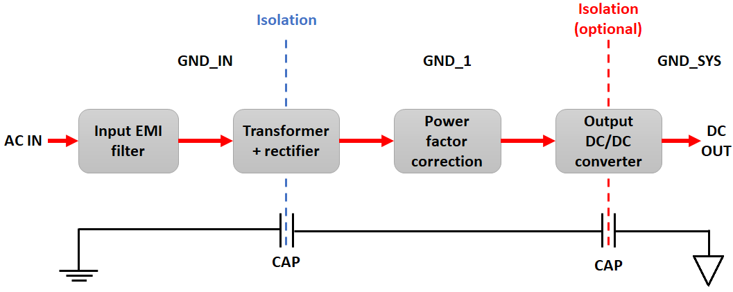
The above block diagram could be implemented on multiple boards, although it’s common to put everything on one board to leave some room for large transformers, heat sinks, fans, and mechanical mounts, especially for high voltage/current power supplies. If you’re designing a small regulator for a board that will plug into a power supply unit, then you’ll be working within the above topology anyways, you’ll just have a ground tie between the output regulator and your new regulator. Again, this is common for high current power supplies.
There are some other points to discuss in the above diagram:
Galvanic Isolation
In the above block diagram, we have three separate ground regions tied back together with caps. Don’t blindly follow this guideline with caps: there is no single PCB grounding technique that addresses every noise source and you should be careful with the above use of caps. This is shown to illustrate one method for ensuring consistent ground potential across all ground regions; this is one recommended method for grounding in industrial Ethernet systems. The idea here is to block any DC potential that may develop between two ground sections
The danger here is creation of ground loops and common-mode noise, which must then be filtered. Tying the grounds together in this way is basically what is done when you have a metal chassis, while plastic enclosures will leave grounds isolated. This gets tricky and requires careful circuit design and PCB layout to still pass all EMC tests.
Output Stage
Galvanic isolation on the output stage is not required; it depends on the DC regulator’s topology (see the flyback converter for a good example). It’s also common to put a conducted EMI filter circuit or common-mode choke on the output to suppress common-mode currents reaching the load circuits. Aside from these points, the output regulator stage will be laid out using best practices for the particular regulator topology. I’ll cover these broader ideas of regulator layout below.
The output stage of the power supply unit may not be the final regulator in the system. Instead could feed another regulator or series of regulators, each of which will provide a set voltage at some maximum current to a group of components. Again, this could be done on a single board, or on multiple boards (one for the power supply, another for the regulator stages):

The above power tree shows regulators in parallel (daisy-chained), but these could also be cascaded in a tree topology. This mapping out of current in your PDN is quite useful as it helps you quickly plot out how much current each downstream regulator stage will contribute to the total current in the PDN. The total current and individual currents will then determine the size of the power rails or power plane needed to carry sufficient current to each section in the system.
Laying Out Each Circuit Block
Now that we can see the overall system architecture, we can get a sense for how to lay out each circuit block in a switching power supply and the overall system to ensure low EMI and safety. Think about the entire block diagram when creating your PCB layout:
- Layout in sections: Much like other boards with multiple functional blocks, try to layout the power supply board in sections. It’s okay to do this in a linear fashion progressing from the input to the output in the block diagram.
- Plan to layout with feedback: Sometimes, such as in precision high current regulators, you’ll have some feedback between sections. Use optocouplers to bridge the ground gap between each section.
- Follow ground return paths: If there is any guideline that is universal in PCB design, it is probably “follow your ground return path.” For power supplies, this is critical for identifying locations where common-mode currents can develop and for ensuring low loop inductances in each supply section.
- Pay attention to high current and high voltage rails: Designing for high voltage and high current are sometimes intermixed. The maximum potential difference between two conductors will determine their minimum spacing (see IPC-2221), and the current a conductor carries will determine its required width to ensure low temperature (see IPC-2152 for internal layers or for external layers).

While working through the PDN design portion, you should also think about how each section will be grounded and how grounds might be tied together to give a consistent reference potential. This is quite important for preventing EMI, as I alluded to above. This should be done before you start working the PCB layout.
Power Supply Switching Regulator Layout Tips
Once you’ve selected components for the regulator, created schematics, and designed a grounding/power distribution strategy, you can start to think through the PCB layout. PCB layout for a switching power regulator is all about tradeoffs: you need to balance conductor sizing vs. clearance requirements, but you need things to be compact.
We’ve posted multiple guides on this blog about laying out specific regulator topologies. Instead of running through all of these possibilities, the list below shows some broad guidelines that will apply in your system.
- Always implement minimum clearance and trace width rules for your system.
- Keep any feedback lines for voltage/current sensing short with the most direct routing possible.
- You’ll probably have to cluster some control and sense components around your driver and controller ICs, so make sure to make short connections between them; it’s okay to cluster these components in a tight area (see below).
- Consider thick copper or even a metal-core PCB if you’re designing for high current.
- Don’t be afraid to use polygons as mounting pads for components or connectors. Be careful with tying directly back to a plane as you may need thermal reliefs.
- Even though regulators can have very high efficiency, they can still get hot. Be sure to make room in the layout for any heatsinks (if any) on ICs. Another option is to use a thermal interface material.
The specific layout guidelines for your switching regulator will depend on the topology, component count, presence of feedback, and grounding strategy. Hopefully, you’ve thought about grounding to prevent EMI and provide any required isolation before you’ve started your PCB layout. To see some more specific guidelines for your specific regulator, take a look at some of these other resources:
- How to Design a Boost Voltage Regulator
- Isolated vs Non-Isolated Power Supplies: The Right Choice Without Fail
- LLC Resonant Converter Design and PCB Layout
- Low Noise, Low EMI Voltage Regulator
What Haven’t We Covered?
Obviously, there is a lot to consider in the above list of layout guidelines for switching power supplies and regulator circuits. So what’s missing? There are a few critical aspects of power regulation and delivery that are not present in the above discussion:
- PDN impedance: If you’re not designing with high speed/high frequency components, you probably don’t need to worry about PDN impedance. Just make sure to use fat power rails and plenty of ground pour. If you are designing for high speed/high frequency, then low PDN impedance is very important for suppressing ripple, which is normally accomplished with plenty of decoupling capacitors and high interplane capacitance.
- Power supply EMI: I’ve alluded to this above. Anytime you create a PCB layout, you should be thinking about ensuring low EMI, but there is a lot that goes into suppressing EMI and passing EMC tests beyond low loop inductance routing. I’ll discuss some of these points in an article dedicated to power supply EMI.
- Analog power: Here, we’re looking at switching converters as normally discussed in the context of digital ICs. What about analog components? Their power needs can be quite different. Digital ICs that source an analog/RF signal will normally do so internally. However, there are specialized LDOs (e.g., NCP161BMX280TBG) or switching regulators (e.g., LTC3388IMSE-1).
There’s also the matter of component selection, such as inductor selection to ensure low EMI and common-mode noise coupling, as well as to ensure low ripple current. The last point in the above list is also quite important because purely analog circuits will not have the same layout style as a power regulator or embedded power supply for digital systems. Once you’re working at extremely high frequencies, RF power supply problems are more difficult to manage due to parasitic capacitance, similar to what is seen in unstable amplifier circuits. This is another topic that I love, but I’ll leave for a different blog post.

With the best PCB design tools in Altium Designer®, you can implement the layout guidelines for switching power supplies I’ve outlined here. You’ll also have the tools you need to find regulator ICs, components for larger regulator circuits, and other components for your system. For more advanced calculations involving conducted or radiated EMI, Altium Designer users can use the EDB Exporter extension to import their design into Ansys field solvers. This pair of field solver and design applications helps you verify your layout before you begin a prototyping run.
When you’ve finished your design, and you want to release files to your manufacturer, the Altium 365™ platform makes it easy to collaborate and share your projects. We have only scratched the surface of what is possible to do with Altium Designer on Altium 365. You can check the product page for a more in-depth feature description or one of the On-Demand Webinars.

About Author
Related Resources


Related Technical Documentation


Take advantage of the world's
most trusted PCB design system.
One interface. One data
model. Endless possibilities.
Effortlessly collaborate with
mechanical designers.
The world's most trusted
PCB design platform
Best in class interactive
routing
View License Options
Thank you, you are now subscribed to updates.