RF Power Supply Design and Layout Guide

One thing is certain: power supply designs can get much more complex than simply routing DC power lines to your components. RF power supply designs require special care to ensure they will function without transferring excessive noise between portions of the system, something that is made more difficult due to the high power levels involved. In addition to careful layout, circuitry needs to be designed such that the system provides highly efficient power conversion and delivery to each subsection of the system.
Very high power systems are still being designed with discrete components that may be connected in a large housing or cabinet, but smaller power systems can be placed on a PCB with some newer components and power regulation strategies. Challenges in these systems fall into two major areas:
- Heat generation in FETs and amplifiers, which motivates the use of advanced semiconductors like GaN on SiC for RF amplification
- Parasitics that could allow high power to leak into nearby circuits along the power feedline, which requires careful placement and routing
The first point happens on the front end when components are selected for power circuits and placed into your schematic sheets. The 2nd point above is where layout and routing become more important. We’ll cover a bit of both areas in this article so that newer RF designers can get their stackup and placement completed before routing.
Starting Your RF Power Supply Design
From the perspective of circuit design, RF power supplies require some of the same regulation and filtration stages as any other power supply intended for a DC system. The main role of an RF power supply is to provide power to an RF system at the frequency of interest, which includes standard components used to generate and condition an RF signal (oscillators, active filters, amplifiers, etc.). The power supply also needs to be able to respond to modulation. In addition to accommodating modulation, an RF power supply design should share some of the same requirements as a typical RF circuit board, namely low loss at high frequencies, as well as sufficiently high temperature ratings and thermal properties.
The block diagram below shows at a high level how to generate RF power at high frequencies.
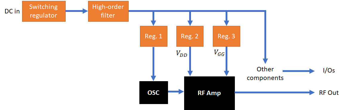
RF power supplies also operate in the inverse, where they receive an RF signal and rectify it down to a DC voltage. This requires building an RF rectifier circuit, which we won’t look at so much in this article as it can be rather involved. Instead, we’ll focus on the RF sourcing aspect.
Regulators and Filtration
RF power supplies that need to source at high frequencies, meaning high MHz or GHz, are typically built from discrete components. However, you can put all of the above sections on the same board. The first step is regulator selection and filter design. In the above block diagram, the higher order filter and switching regulator need to be built to follow the envelope of any modulated signal (for AM output), or to modulate its output at the baseband frequency (for FM output). This might require a multiphase, multilevel topology for your design; read this article to learn more about the regulator and filter portion of the design.
In selecting any downstream regulators (these could be switching or LDOs), be careful to watch out for the efficiency. If you’re using an LDO, the voltage differential should not be too high as this will drop a lot of power over the LDO, and the high thermal resistance of the component can cause it to quickly heat up above its temperature rating. In a recent prototype my company built, we opted for LDOs with conduction cooling via the enclosure. If you need to drop down the voltage by a large amount, you should use a switching regulator and apply another higher order filter to ensure low noise is given to the VDD port, VGG port, and oscillator.
How to Handle Ground
Just like any other mixed signal design, don’t try and galvanically isolate your switching regulator output (if you’re using one) from the RF section by routing over split grounds. You’ll create the same type of EMI problem you would see when a single-ended digital signal is routed over a gap in a ground plane. This is a common mistake in mixed signal systems, and it’s easy to make the same mistake in an RF system by assuming that the output from the switching regulator is purely DC. Even with envelope tracking, you’re still drawing your time-averaged power at the baseband frequency, which could be on the order of tens or hundreds of MHz.

Keep uniform ground and practice good placement while maintaining impedance control on coplanar lines, rather than trying to take the easy route and splitting up your ground layer. If you can place the RF components in their own sections, and place the DC/regulation components in their own sections, you can prevent interference between them as long as you can properly track return paths.
Stackup Design and Material Selection
When designing your stackup, you’ll need to consider the operating frequency for your regulator and the length of your RF lines on the board. For longer RF lines, you’ll need to use a low loss laminate, possibly a PTFE laminate. RF power supplies that aren’t routing long lines, or if you’re just not worried about losses, you can usually get away with FR4 laminates as stackup materials. One way to compromise low loss and low cost is to use a hybrid stackup with a low-loss dielectric supporting your RF lines.
The above example with power rail routing over ground can be done on a 4-layer board as long as you also route RF lines on a surface layer. You could also use a uniform ground and a power plane to provide power from the regulator section to the components, and route the RF lines on the surface layer to maintain a 4-layer board. This is a good way to use a hybrid stackup with low-loss PTFE on the surface layer. However, the only isolation you can reliably achieve in this board comes from coplanarity in your routing, i.e., from the via fence you place around RF lines and around components to prevent noise coupling between board sections.

You could also use a 6-layer or 8-layer stackup for this type of design when you need to work with higher powers while also providing high isolation. For example, you could make L3 a signal layer for coplanar RF lines between two GND planes (on L2/L4), then place power on L5, and possibly route any other signals you might need on the surface layers or L6 (see below). This is better for a high power design that requires a lot of isolation as the ground plane will provide shielding between layers.

By providing isolation between different sections of the design, you can help prevent the type of parasitic coupling that allows noise to propagate into the output. The output from the supply should have sufficiently low noise and distortion to provide clean power to other components. There are two main sources of noise in this type of design:
- Noise from the switching regulator or a noisy DC input.
- Noise coupling back to the amplifier input from the output
Both points are solved with the stackup design tips mentioned here, as well as with smart placement of the noisy sections away from the RF output section. The second point is more challenging at higher frequencies, and it is possible to see the RF output experience positive feedback by coupling back into the input of the amplifier stage. Routing and filtration are also quite important as these can help provide additional isolation and noise elimination.
Placement and Routing
These two aspects of the design are critical as you need to suppress the noise problems I mention in the above two points. Route the RF traces from the oscillator, through the amplifier, and to the output as grounded coplanar waveguides (either on the surface or on internal layers) to ensure there is some isolation. Don’t use guard traces to provide any shielding as they will create more noise coupling; only use the via fence style that you calculate for your coplanar lines. Also, make sure that if you do route on an internal layer, to determine whether you need backdrilling by analyzing your via stubs.
Any other conditioning that might be required on the output depends on the function of the supply. Will it route directly to an antenna, or to an SMA/u.FL coaxial line? It’s typical to put the RF output through a filter (either a BAW or SAW filter), although be careful with component selection as chip-packaged BAW and SAW filters can’t always accept the high RF powers used in some RF power supplies.
One other component you might need on the RF Out net include an isolator/circulator to prevent any reflection from traveling back to the amplifier. There are some SMD isolators you can use on the output, which is particularly important if you’re implementing power over RF or sending your RF output directly to an antenna.

If you do need to route any signals through an external RF module, you can place SMD u.FL or SMA connectors to make these connections. You can take the signal off the board, through the module, and back onto the board as needed in the event your power level exceeds the allowed value for an equivalent SMD/through-hole component on the board.
In Summary
While RF power amplifiers and power supply designs have typically been built from discrete filter elements, newer components allow you to be very aggressive with your form factor and consolidate many of these elements onto a single board. And of course, make sure you consult your fabricator about your stackup to ensure it’s manufacturable as a hybrid board. Also make sure you account for copper roughness and dielectric dispersion in your transmission line design to ensure your RF transmission line impedance has the typical 50 Ohms value.
When you need the best PCB tools for RF power supply design, look to the complete set of PCB design, layout, and simulation features in Altium Designer®. After you complete your physical RF power supply layout, you can use the EDB Exporter extension to import a design into Ansys field solvers and perform a range of SI/PI/EMI calculations for your design. When you’ve finished your design, and you want to release files to your manufacturer, the Altium 365™ platform makes it easy to collaborate and share your projects.
We have only scratched the surface of what’s possible with Altium Designer on Altium 365. Start your free trial of Altium Designer + Altium 365 today.

About Author
Related Resources


Related Technical Documentation

Table of Contents
Take advantage of the world's
most trusted PCB design system.
One interface. One data
model. Endless possibilities.
Effortlessly collaborate with
mechanical designers.
The world's most trusted
PCB design platform
Best in class interactive
routing
View License Options
Thank you, you are now subscribed to updates.