RF Signal Chain and Link Budget Basics

Table of Contents
IoT devices deployed in the field will generally have two means to talk to each other: over a cable or wirelessly. In wireless communication, there is a quantity used to describe how much power arrives at a wireless receiver: the link budget. In a wireless system connecting two devices, the link budget is intended to account for all sources of gain and loss that will impact power delivery to a receiving antenna. If you're designing a wireless IoT device, and you know how to calculate the link budget, you can reasonably estimate whether your signal will reach its destination and be read by the receiver.
To calculate the link budget, the designer needs to know something about all other sources of gain and loss in the system. Once link budget is determined, the designer can judge whether some modification is needed in their RF signal chain. Such modifications could include swapping material sets, redesigning a stackup for lower loss, adding amplifiers and filters, or modifying existing elements in the signal chain.
To help you determine the link budget in your system and whether your RF signal chain needs an upgrade, I've provided three tools in this article:
- The link budget formula
- A link budget calculator
- The free space path loss formula
With these tools you can calculate your link budget and determine if any additional components are needed along your RF signal chain. Knowing the link budget and comparing the received power to the receiver sensitivity will also help designers determine whether their signal chain needs modifications. I'll outline the potential modifications your system might need in this guide.
What is the Link Budget For an RF System?
The link budget in an RF system gives an estimate of the power one would expect to arrive at a receiver given all possible sources of gain and loss along a wireless link. The topology of an RF system with its link budget is shown below:
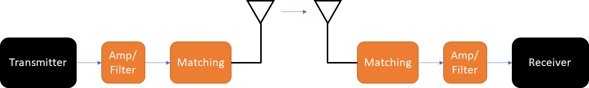
Along the link, there can be amplification (built into the transmitter/receiver or placed as an external component), and there will be losses from the materials and other components used in the system. A link budget calculation intends to account for these losses and gains in the system as a signal is transmitted to a receiving device.
Link Budget Definition
The link budget in a wireless system is defined in the following formula:

In this formula, the losses have a negative sign on them, so a loss would be placed in this formula as a positive decibel value. The various terms in this formula are defined as follows:
- Pt - Transmitter power output, or the equivalent power that would be radiated isotropically with no antenna/amplifier gain
- Gt - Transmitter gain, accounting for the antenna gain and any amplifier gain
- Lt - Signal chain loss on the transmitter side
- Lfs - Free space path loss, or the power lost during propagation between the transmitting and receiving antennas
- Lm - Miscellaneous losses, or any other losses not included in this formula
- Gr - Receiver gain, accounting for the antenna gain and any amplifier gain
- Lr - Signal chain loss on the receiver side
The transmitter power is the power output to the signal chain in the transmitting system. Once the signal begins propagating in the PCB and to the transmitting antenna, it could experience any of the standard loss mechanisms along the interconnect,
Free Space Path Loss
The free space path loss (Lfs) listed above defines the expected loss along the propagation path between the two antennas of the transmitting and receiving devices. The path loss in air depends on the frequency and distance between the two devices:

The terms in this equation are defined as:
- FSPL - Free space path loss, measured in dB
- d - Line-of-sight distance between the transmitter and receiver, measured in km
- f - The carrier frequency for the transmitted signal, measured in MHz
This equation does not account for important factors in propagation, such as absorption or scattering losses through air, or the presence of any obstructions along the propagation path (such as buildings). These factors can significantly increase the free space path loss.
Link Budget Calculator
To get a quick and easy estimate of the link budget in your system, I've created the following calculator that includes all lossy factors in a typical link between two devices. This calculator returns the estimated signal strength that arrives at the receiver, in dBm. The power output here follows the definition given above: it refers to the power given to the antenna that would have been radiated isotropically (with antenna gain = 0 dBi), but instead could be focused with a directional antenna. Remember, antenna gain is directional, so your calculation will only be valid along certain directions.
The calculator uses positive sign convention, as defined in the formula shown above.
The result can then be compared with the receiver's sensitivity rating. If the calculated result is less than the receiver sensitivity, then the losses in the system should be reduced, the gains should be increased, or the devices should be brought closer together.
How to Increase Link Budget
When it is found that the system's link budget value as calculated above is too low, the link budget needs to be increased so that the receiver in your device can read the received signal. The simplest way to increase the power sensed at the receiver is to apply changes to the PCB and the RF front end:
- Apply amplification between the transmitter and the antenna (or between antenna and receiver)
- Use lower loss materials
- Use an antenna with higher gain (directivity)
- Place the devices closer together (reduce d)
- Change the stackup to reduce losses on controlled impedance lines
Some designers will start by trying to decrease losses on the PCB by using a lower-loss material. In sub-GHz ranges, the material loss will already be very small (both from the dielectrics and from copper, as I've shown in this article on copper roughness). At higher frequencies (above 5 GHz), low loss materials (both copper and dielectrics) can have a substantial effect on decreasing losses in the RF signal chain.
Transmit-Side Amplification
There is a tendency in some RF applications to simply accept the amplification that is built into the transmitting device. These devices have a power amplifier built into them that sets the power output to the value that is supplied in the component datasheet. These amplifiers are often running near saturation and there can be some harmonic content with intermodulation products present on the signal. When designing a signal chain, an amplifier can be placed in the signal chain that will provide extra amplification along the signal path, and this will increase the amount of power sent to the antenna.
On the transmit side, because the transmitter has high power output, a broadband signal fed into a power amplifier can cause the amplifier to run near saturation. The result is generation of intermodulation products, which will occur when the amplifier's transfer function begins to run nonlinearly. This is a problem in frequency-modulated signals, but it will also happen in broad-band signals generally. An example showing intermodulation product generation for a frequency modulated signal is shown below:
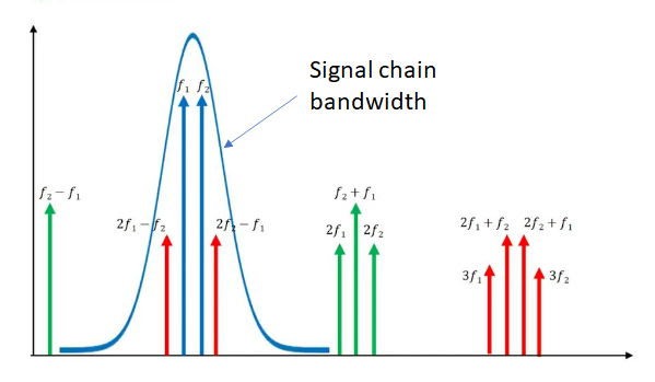
The problem with these peaks is that they are difficult to filter, and they can increase faster than the main signal. This is illustrated in the typical power amplifier transfer curve shown below. To prevent this intermodulation product generation, we normally set the 1 dB compression point as the limit for input power (in dBm) in a power amplifier.

Receive-Side Amplification
In the above description, I've focused on amplification on the transmit side, but you could also apply amplification on the receive side. This would require placing a low-noise amplifier (LNA) in the signal path that is tuned to the operating frequency and has enough bandwidth to uniformly amplify the entire signal. As long as the signal in the receiver-side signal chain is intense enough, it can be detected above the noise floor in the system.
On the receiver side, you're much less likely to run the amplifier or the receiver's input near saturation simply because you don't need to. There are two reasons for this:
- The signal power on the receive side will probably be very low, which is why you would try to apply amplification in the first place. This means the LNA is less likely to run at saturation
- The signal on the receive side does not require huge gain; it only needs to have enough gain to exceed the receiver sensitivity threshold.
As long as you can exceed receiver sensitivity threshold at the specified distance requirement, then you will have applied just enough gain. However, you have to balance this against the maximum receiver input specification as this tells you when the receiver input starts to saturate. If the receiver amplification is too high, then you will have a minimum distance requirement to enforce! Balance receive side amplification carefully as it can cause a system to work incorrectly.
At High Frequencies (>5-10 GHz), Use Wider 50 Ohm Traces
One option to reduce losses is to apply changes to the stackup so that transmission line losses can be reduced. If you increase the outer dielectric thickness slightly, this would force you to increase the line width, which will reduce the DC and skin effect losses at high frequencies. This is also appropriate above ~5-10 GHz, and the loss reduction will be considerable at very high frequencies reaching the mmWave range. This strategy could be used with hybrid stackup design using low-loss PTFE materials to reduce losses significantly.
When All Else Fails, Change the Distance
Eventually, all the possible improvements in the signal chain devices will have been applied, and the two devices simply won't be able to operate at the desired distance given their operating capabilities. In this case, you will have to reduce the distance between the two devices as this will reduce the free space path loss. If you manage to get your hands on more sensitive receivers, higher saturation amplifiers, and higher directivity antennas, then you can continue to increase the distance between the devices.
When you need to design your RF PCB to properly carry signals and maintain a sufficiently high link budget, use the complete set of PCB design tools in Altium Designer®. When you’ve finished your design, and you want to release files to your manufacturer, the Altium 365™ platform makes it easy to collaborate and share your projects.
We have only scratched the surface of what’s possible with Altium Designer on Altium 365. Start your free trial of Altium Designer + Altium 365 today.

About Author
Related Resources


Related Technical Documentation


Take advantage of the world's
most trusted PCB design system.
One interface. One data
model. Endless possibilities.
Effortlessly collaborate with
mechanical designers.
The world's most trusted
PCB design platform
Best in class interactive
routing
View License Options
Thank you, you are now subscribed to updates.