Routing Differential Pairs in a PCB Layout with Altium Designer

Table of Contents
- Defining Differential Pairs in Your Schematic
- Which Classes to Define?
- Routing Differential Pairs in Your Layout
- Define an Impedance Profile
- Defining Design Rules: An Individual Pair
- Defining Design Rules: Multiple Pairs
- Setting Additional Design Rules
- Routing Differential Pairs in the PCB Editor
- Next Steps: Length Tuning and Signal Integrity
If you’re working with a high speed device, you’ll likely need to route differential pairs between components. Many high-speed PCBs include differential interfaces that require specific odd-mode/differential impedance values, and the PCB layout designer will have to specify those geometry constraints in their PCB Editor to ensure traces have the right impedance values.
The fastest and most accurate way to do this is to fuse the impedance calculation and design rule setup into a single workflow. Altium Designer helps you do this with the Layer Stack Manager feature, which will pass its calculation result to the PCB Rules and Constraints Editor. Other features such as decoupling length limit, total trace length limit, and length/delay mismatch limits.
Defining Differential Pairs in Your Schematic
When you need to use differential pairs in your device, you’ll need to define which nets will use differential signalling to interface with your components. Simply placing a net is not enough, a net needs to be specifically called out as being part of a differential signal. The schematic and layout editor in Altium Designer® include net definitions functions, and you can define differential pairs within a signal net. First, you’ll need to select some components that will communicate with each other, place them in your schematic, and define which ports will use differential signalling.
Here, we have three objectives:
- Define differential pairs in the schematic;
- Setup impedance and routing rules for our differential pairs;
- Start differential pair routing in the PCB layout.
To get started, we’ll look at the schematic below and define the differential pairs we need to use create our differential signal. This schematic contains a Microchip LAN9514I-JZX USB/Ethernet Controller, an edge connector, and a few shielded USB connectors. These component can be found in the Manufacturer Part Search panel within Altium Designer. For brevity, we’ll only look at “Part A” from this pin list, labeled with the designator “U1A” on the schematic. Some of the outputs will be connected to the board edge connector, and other nets will be routed to USB connectors.
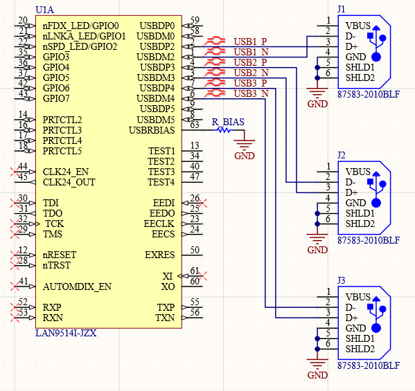
USB/Ethernet controller and some connections in Altium Designer
Note that, in this schematic, I've defined the USB outputs as differential pairs with a special directive symbol. you can specify which connections are differential pairs by clicking on the “Place” menu. Highlight the “Directives” option and select “Differential Pair”. You’ll be able to place the directive symbol on the connections you want to function as differential pairs. Simply select all nets that will be part of a differential pair.
Next, each half of a differential pair is defined as positive or negative using its net name. The positive end must be named using “_P” at the end of the net label, and the negative end must be named using “_N”. I've done this for the USB1-USB3 lines in the above schematic. We can do the same for the RX lines in the lower left portion of U1A. Note that these would normally be connected to a magnetics and Bob Smith termination circuit before being routed to an RJ45 connector, but we'll just use the simple situation above to illustrate differential pair routing.
Which Classes to Define?
Routing your differential pairs successfully requires setting up Differential Pair Classes and Net Classes. The goal here is to group multiple pairs together so that the same design rules can be applied to all pairs in the group. This group is a Differential Pair Class, and you'll apply geometry requirements and length matching requirements in the Design Rules editor.
Since we need to define a Differential Pair Class, we’ll add this to each directive. I’ve defined classes USB1 o USB 3 for each of the connections shown in the schematic. If you double click on the directive symbol, you’ll be able to define classes and design rules for a connection in a differential pair. You can also right-click on the directive symbol and click on “Properties”. This will bring up a dialog that allows you to specify a label, classes, and rules for a differential pair. Here, we will add the “Diff. Pair Net Class” to each pair and assign a class name for this net. This is shown below for USB1_P.
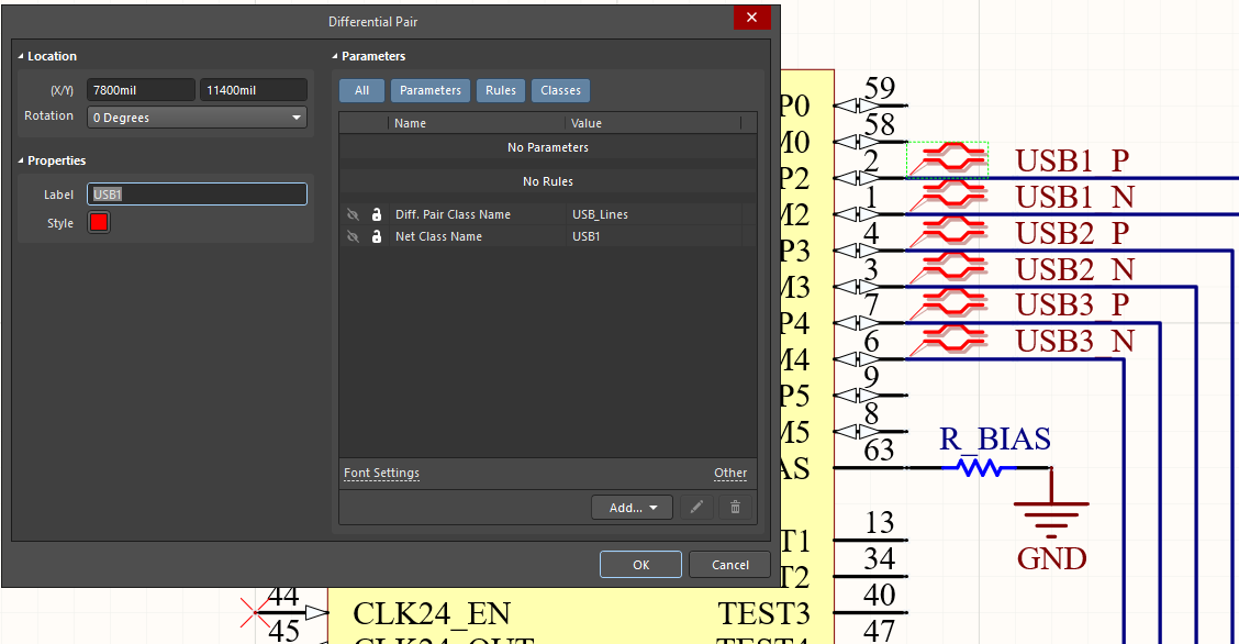
Defining a differential pair net class
You'll also need to add design rules to this directive. This can be done within the dialog shown above to apply a design rule to an individual net. If you want to do something like length tuning for a differential pair, or for a group of differential pairs, it's better to do this in the PCB Editor. If you create a rule from the above dialog, a new design rule will be created that only applies to this net. Since we want to apply length matching to individual USB1 to USB3 connections, we can just define the Differential Pair Classes shown above and wait until the schematic is captured to set a design rule for these nets.
Routing Differential Pairs in Your Layout
Define an Impedance Profile
Before you capture your schematic and start routing, you need to create a new PcbDoc that includes an impedance profile for your differential pairs. For this simple example, I've created a 4-layer PCB with a single-ended impedance profile (50 Ohm, named S50) and a differential pair impedance profile (90 Ohm, named D90). The differential pair impedance profile will be used for the USB lines as these need to have defined differential impedance. You can do this through the Layer Stack Manager within the PCB Editor. My stackup and impedance profile are shown below.
Note that I have defined the spacing between the traces in the differential pair to be the default value of 5 mil. However, you might consider changing this, read this article for guidance on setting your differential pair trace spacing.

Defining an impedance profile for differential pair routing
Defining Design Rules: An Individual Pair
At this point, we can capture the schematic as a layout and route the differential pairs we defined. I’ve defined differential pairs for the rest of the connections between the FPGA and the connector. First, add a new PCB to your project and capture your schematic. You can do this by opening your empty PCB and clicking the “Design” menu, followed by “Import Changes From…”. Note that a Room will be created by default unless you uncheck the option in the Engineering Change Order dialog.
Before routing, we need to define design rules for the differential pair nets in our schematic. This is done by opening the Design -> Rules dialog in the PCB Editor. Here, we need to define the following rules for these nets to comply with the USB specification:
- Length tolerance: 2 mil (found in the High Speed -> Matched Lengths entry)
- Differential pair routing constraints: defined by impedance profile (found in the Routing -> Differential Pair Routing entry)
When you define the design rules for these pairs, you can create a rule for each net and select the impedance profile you want to use. This is shown below.
Defining design rules for individual nets
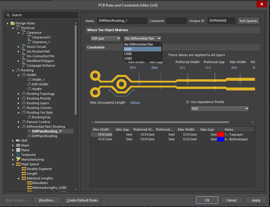
Defining Design Rules: Multiple Pairs
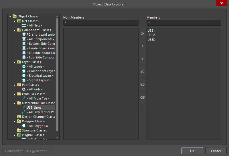
Since we're working with multiple differential pairs that all need the same design rules, a better option is to create a single design rule that applies to our Differential Pair Class. To check and create classes, open the Design -> Classes dialog in the PCB Editor. Go down to the Differential Pair Classes entry, right-click, and create a new class. As long as you defined your differential pairs correctly in the schematic, you can now add these pairs to your new class. This is shown in the image below.
Defining a class for a group of USB differential pairs
Now, you can go to the design rules editor and select the net class you just created for the length tolerance and routing constraints, just as was done for individual nets. Under the "Where The Object Matches" entry in the design rule window, select the Differential Pair Class you defined in the above window. The design rule will now apply to all nets in the class (USB1, USB2, and USB3). This will apply the impedance profile you defined in the Layer Stack Manager as long as you select the option in the design rule window.
Setting Additional Design Rules
Additional design rules that might be required to ensure consistent impedance and maintain singnal integrity include:
- Total routing length: This is primarily related to the total insertion loss that is allowed along the differential pair.
- Maximum mis-matched length: A length mismatch impacts mode conversion, and high-bandwidth interfaces will require limits on mode conversion. Length mismatch is also required to create margin for skew along the net.
- Maximum via count on net: Each via has the potential to create additional return loss due to impedance mismatch, so it might be desirable to limit the number of vias.
- Routing layers restriction: Differential impedance profiles are defined for all signal layers and will be enforced on any signal layer. If you like, you can restrict your differential pair routing to specific layers.
- Maximum stub length: The maximum stub length is more important in interfaces/channels with multi-GHz bandwidths.
- Return path: The allowed deviation from GND nets on a neighboring can be set and detected during routing.
Most of these rule settings can be found under the High Speed section of the PCB Design Rules and Constraints Editor.
Routing Differential Pairs in the PCB Editor
Now it's time to import changes from the schematic and start your PCB layout. We've done a lot of work on the front-end to set the constraints before creating the PCB layout, but now the design rules we have set up will ensure the routed traces will have the required impedance, spacing, and length matching rules as the pairs are routed. Once you've arranged the components the way you want, select the Interactive Differential Pair Routing option at the top of the PCB Editor window.
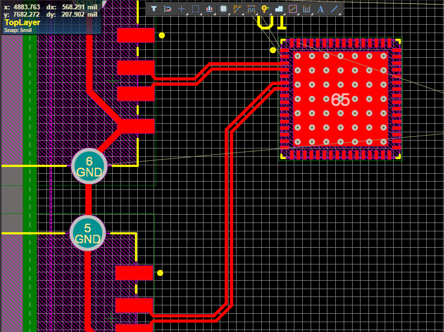
The image below shows the component we want to work with in mid-route. When you use the interactive router, you only need to click on one end of the net, and both traces will be routed in tandem as you move across the board.
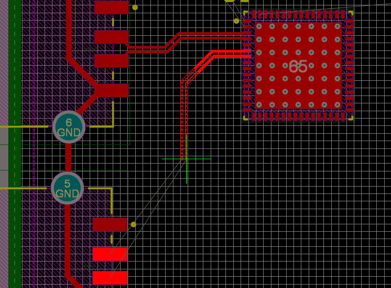
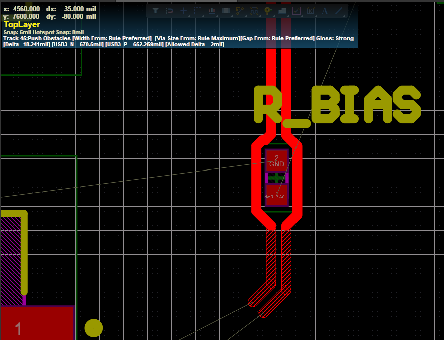
While it's not ideal to allow obstacles to fall between the traces in your differential pair, the router can automatically move the traces around the obstacle during routing. To illustrate, a resistor has been placed in the routing path as shown below. As the traces approach the component, they'll be automatically moved around the component with the tightest possible clearance. You can then click on the far side of the component to set your routing around the component, and you can continue routing towards the destination.
Note that this may trigger a design rule error for the maximum uncoupled length, but generally obstacle avoidance will be followed here as you move around the component.
For more complicated components, such as BGA with high ball count or an SMD connector with narrow pin pitch, you'll need to use a fanout strategy to create connections for your traces. Additional routing settings into these components can be controlled by creating a Room object around the component. You can then specific constraints, such as clearances, inside this region using the "Within Room" custom query when defining design rules. This allows you to control neck-down between pins, decoupling lengths, parallel segments, and clearances only inside the room region, which minimizes any impedance mismatches looking into component pinouts.
Next Steps: Length Tuning and Signal Integrity
The image below shows two routed differential pairs. This is a quick and easy process thanks to the interactive routing tools in Altium Designer. At this point, you can apply length tuning to each pair, or across multiple pairs. Take a look at this article to see how to apply length tuning to differential pairs.
Finished differential pair routing in Altium Designer
You could also use the xSignals package to examine signal integrity for these nets, or for a group of nets. Examining a group of nets requires defining an xSignals class from the Design -> Classes dialog, just as was done for creating a Differential Pair Class. This allows you toe examine the rising and falling edges of signals, and any overshoot/undershoot. Other high speed design rules can be applied to this layout inthe same way as was done for length tolerance and differential impedance. The design rules shown here are the key to quick and easy differential pair routing.
Altium Designer unifies information in your design with your routing tools, ensuring that your next device will function as intended. The integrated environment in Altium Designer allows all your tools to communicate using the same rules-driven design engine. The best schematic, CAD, simulation, and routing tools are exactly what you need to create the best PCBs.
Talk to an Altium Designer expert today if you want to learn more about Altium Designer.

About Author
Related Resources


Related Technical Documentation


Take advantage of the world's
most trusted PCB design system.
One interface. One data
model. Endless possibilities.
Effortlessly collaborate with
mechanical designers.
The world's most trusted
PCB design platform
Best in class interactive
routing
View License Options
Thank you, you are now subscribed to updates.