Should Ground Be Placed Below Inductors in Switching Regulators?

Table of Contents
We love answering questions from our readers and YouTube viewers, and one of the recent questions we received relates to EMI from switching elements in a switching regulator:
- Should a cutout be placed below the inductor in a switching regulator circuit?
This is another one of those “it depends” questions as it relates to the type of inductor being used in the design, the coil orientation, and whether magnetic flux leakage from the inductor is large enough to create a noise problem. There are different types of inductors with different form factors, and these inductors can produce different magnetic field profiles around the component during switching operation in a switching regulator.
Despite the variations in inductors and their magnetic behavior, there are some general principles that can be used to judge the effects of placing ground near inductors in switching regulator circuits. We’ll look at some of these principles in this article.
How an Inductor Couples Noise in a Switching Regulator
When an inductor is operating with a switching current in a voltage regulator circuit, the switching current generates a magnetic field. This is a basic fact of electromagnetism as described in Maxwell’s equations. The time-varying magnetic field can then induce an electromotive force in a nearby circuit.
Let’s consider for a moment the wirewound inductor shown in the 3D view below. When a switching current flows through the coil, there will be a time-varying magnetic field emanating from the coil. If you go back to your physics classes, you’ll know that the changing magnetic field generated by the switching current will induce an eddy current in surrounding conductors.
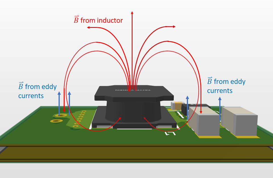
The region with field lines nearly perpendicular to the ground layer on L2 will induce an eddy current.
Different types of inductors will have different distributions of the magnetic field around the inductor core. The orientation of the inductor core, the materials used to build the inductor, and the type of inductor (wirewound, film type, shielded, etc.) will matter as well. In the above case, we have a vertically-oriented inductor coil. However, if this inductor is shielded, the magnetic field generated by the switching current will be mostly contained within the inductor package. Other packages like toroidal inductors help contain flux within the wrapped coil.
Cutouts Still Experience an Inductive EMF and Currents
If you place a cutout, there will still be an EMF and resulting current induced in the nearby plane layer. In the example below, if we assume the magnetic field is pointing into the cutout, then the resulting current loop would be clockwise as shown below.

If we cut this ground through all layers, now we have a very bad situation where we are inducing these currents on all layers. It also allows the magnetic field to emanate around the PCB, whereas the case with GND would normally shield this. This is very bad from an EMC perspective. Placing the ground below the inductor will block this magnetic field from passing through the board and possibly interfering with other components; I think this is an appropriate justification for using it below the inductor.
How the Magnetically Induced Currents Affect Operation
The logic above goes that, if the ground is placed below the inductor, the magnetic field will generate eddy currents on the next layer. These eddy currents will generate their own magnetic field that opposes the inductor’s magnetic field. The reasoning goes that the inductor will have lower “equivalent” inductance because the total magnetic field created by the switching current is lower. If you want, you could also think of this in terms of the mutual inductance between the inductor coil and the plane; this lowers the total inductance of the system.
The supposed result would then be noise that is induced in other circuits. However, the ground provides some shielding with respect to circuits and routing on internal layers, which confines the noise near the surface layer. Whether or not you place the cutout, the eddy current and noise would be there anyways, so you will have to tolerate some noise in circuits near the inductor. Since the better option is to shield against this noise in all other layers, I am in favor of ground below the inductor. Bringing the ground closer to the elements in your power regulator is also a good idea generally for control over parasitics.
Summary
We have a couple main results from the above discussion:
- Placing ground below the inductor lowers its effective inductance; bringing ground closer to the inductor produces greater decrease in inductance
- Placing ground below the inductor helps shield other circuits on internal/back layers from noise directly from the inductor core, but be careful if the switching loops are spread across the stackup as it’s possible to induce noise on nearby traces
In closing, it’s fair to conclude that placing ground below the switching node and inductor in a switching regulator PCB layout is not problematic if you’re willing to sacrifice a bit of inductance due to the presence of eddy currents in the adjacent copper. A better option is to combine this with a shielded inductor; you get the benefit of having ground for shielding and the inductor package will better contain the magnetic field. The issue with noise on the top layer is solved through appropriate layout and additional shielding by placing the GND nets closer to the control circuitry and any sensitive traces. Mark Harris provides a nice example in an older project.
As far as the switching node is concerned, there may be some debate as to whether placing ground near the switching node causes excessive noise coupling away from the switching node and into ground. As long as the rectifying element’s capacitance is large enough, the path of least impedance will be through the rectifying element rather than through capacitive coupling back to the nearby ground plane. In most cases, this is the terminal capacitance of the rectifying MOSFETs.
When you’re ready to build your stackup and route your PCB, use the best set of PCB layout features in Altium Designer®. When you’re ready to share your designs with collaborators or your manufacturer, you can share your completed designs through the Altium 365™ platform. Everything you need to design and produce advanced electronics can be found in one software package.
We have only scratched the surface of what is possible to do with Altium Designer on Altium 365. Start your free trial of Altium Designer + Altium 365 today.

About Author
Related Resources


Related Technical Documentation


Take advantage of the world's
most trusted PCB design system.
One interface. One data
model. Endless possibilities.
Effortlessly collaborate with
mechanical designers.
The world's most trusted
PCB design platform
Best in class interactive
routing
View License Options
Thank you, you are now subscribed to updates.