Should You Route Signals in Your PCB Power Plane?

I often get questions from designers asking about things like signal integrity and power integrity, and this most recent question forced me to think (again!) about some basic routing practices near planes and copper pour. Here’s the (paraphrased) question I recently received on LinkedIn:
I am wondering about your perspective on mingling signal/power on the same layer in a PCB stack-up. Is it okay to route signal traces on the same layer as power planes? I’ve seen some stackup guidelines that suggest this is fine, but no one provides solid advice.
Once again, we have a great example of a long-standing design guideline without enough context. The short answer to this question is “yes,” it is okay to do this in certain situations. This practice is quite common, and we do this on client boards without any impedance problems, EMC problems, or DC power loss on those products because the stackup was designed correctly and because we thought about how to route the design properly. However, there are multiple dimensions to consider when routing signals on a power layer, or when routing power rails on a signal layer. The difficulties come from considerations around power integrity, controlled impedance, and DC power distribution in your board.
How to Route Signals in Your PCB Power Plane Layer
Before you start cutting up your PCB’s power plane layer with traces, you’ll need to think about your design requirements in the following areas:
- Power plane current capacity
- Low-speed vs. high-speed signals and impedance
- Return paths if the plane is used as a reference layer
Let’s look at each of these areas in more detail.
Power Plane Current Capacity
Whenever you design a power plane, it will have some defined current-carrying capacity that is related to the dimensions of copper that makes up the plane layer. If you start routing through a high power plane, you’re carving up the plane into sections, and each section will have lower current capacity than the uniform plane layer. In addition, if the shape of your power layer is very complex, you may end up creating a funnel with high current density that can get rather hot. You can visualize effects like this in a PDN analyzer simulation (see this article for an example).
One solution to make up for routing in a power layer is to use another power plane on an adjacent layer that runs in parallel. In this arrangement, you are essentially splitting the current across two parallel planes, which will help ensure you don’t exceed the current capacity on any one plane section. For most low-power devices, you generally don’t need to worry about this. However, if you have a high-power system, it’s likely you’ll need to do this regardless so that the system can provide enough power without getting too hot. One common example where this is done is in backplanes (3U/6U) or other rack-mount units.
Trace Impedance
If you’re not routing controlled impedance lines through copper pour on your power layer, you won’t need to worry about this so much. Single-ended digital protocols like SPI and I2C, as well as GPIOs, can be routed through copper pour without worrying about impedance because they do not have an impedance specification, but you should still follow the other guidelines in this list (where applicable). High speed protocols where impedance is important are another matter, and you’ll need to ensure you provide enough copper pour clearance around these traces to ensure impedance targets aren’t violated. If your power pour comes too close to your traces, then you need to use a coplanar calculation in your layer stackup to ensure you don’t violate impedance tolerances.
The danger involved in cutting up a plane by applying high clearance is that you end up cutting the copper into too many sections. If you route too many traces, you’ll leave a lot of leftover copper around the layout that is cut up into small sections. With a low layer count board that also requires impedance control, you might not have another power layer to use to tie all these sections back together. If you find that you have to route a large number of traces through a power layer, you might be better off just adding two more layers (power and ground).
Return Paths and Routing Over Power Plane Splits
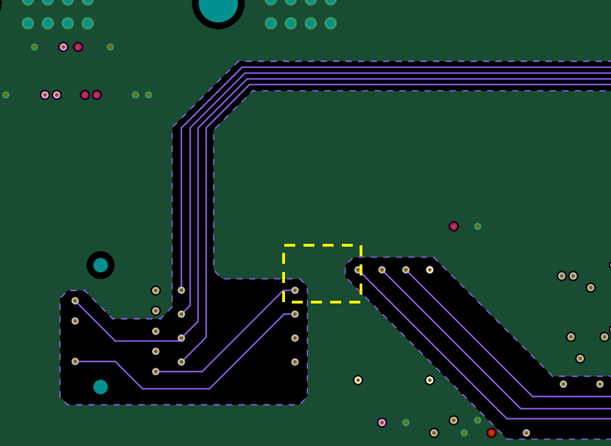
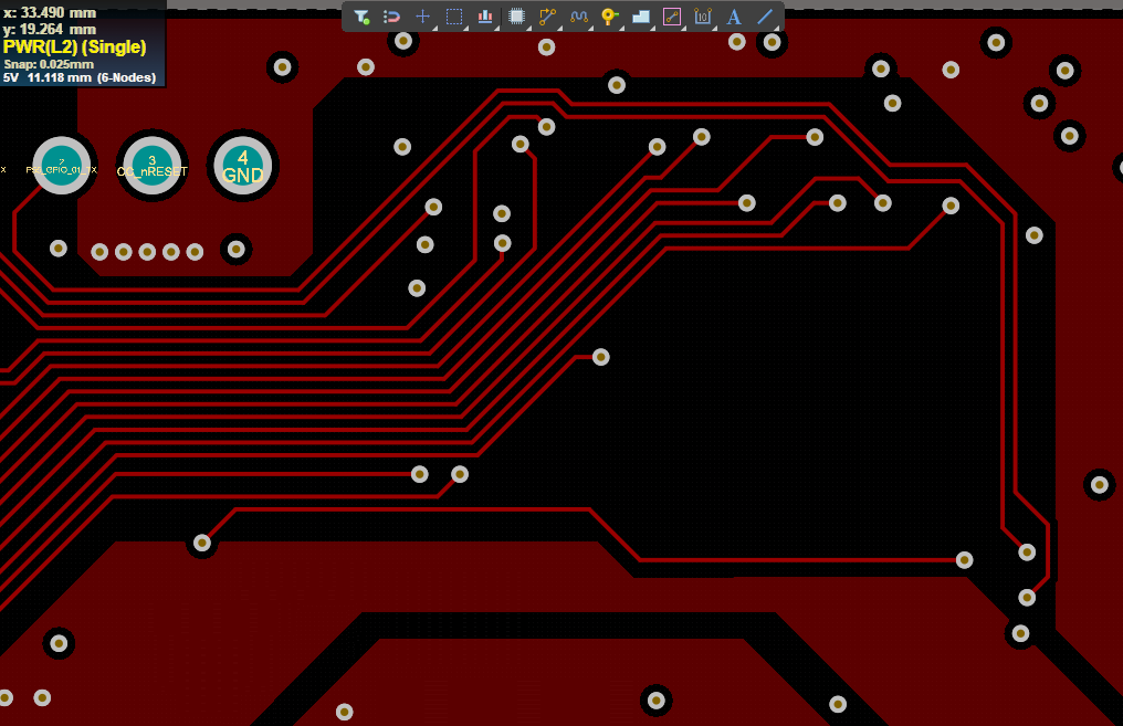
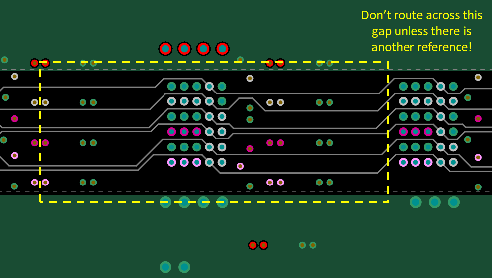
As is the case with routing in any other situation, make sure you have a well-defined return path for signals in your PCB, especially when routing in a power layer. The issue here is if you route in an adjacent layer. When you route in the same layer as your power region, you’re putting gaps in a reference plane. For power regions this is generally fine unless you are using the power region as a reference for signals in another layer. Then, if you should happen to route over one of these gaps, you create a region with higher parasitic inductance, which can then receive more EMI from crosstalk or external sources.
For lower speed protocols propagating between two plane layers, you can probably get away with routing over a power plane split as long as the plane in the other layer is uniform. The impedance discontinuity you create will be electrically short, so you won’t need to worry about reflections, and the presence of the plane on the other layer helps ensure there is still a well-defined return path, despite the higher inductance in the region with the plane split. For higher-speed signals, this is much more important and you’re probably better off adding a new layer to make room for these signals rather than cutting up a power plane.
For higher speed protocols, there is an issue with routing a stripline over this kind of split in a plane layer, as has been pointed out by other authors. Suppose, for example, we route a stripline between a power layer and a ground layer. and the ground layer has a split in it due to routing in the power layer. This would look like the following model (SE stripline width = 8.64 mil, DIFF striplines width/space = 6.223 mil/10 mil).
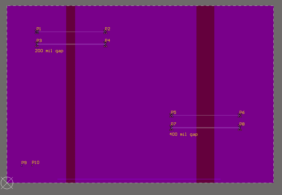
Here I have created a very basic model that can be used in a signal integrity simulation; Signals start from pads on the top layer flooded with ground pour (L1), and there are two splits in a power plane layer (L2) that might be used for routing signals. On the next adjacent signal layer (L3) we have two groups of striplines with defined impedance (50 Ohm single-ended, 100 Ohm differential pair). These signals are being routed over a ground plane on L4. All dielectrics are 10 mil thick with Dk = 4/Df = 0.02. The signal vias have stitching vias added to provide matched input impedance looking into the striplines in each configuration.
From this simulation model, we have the traces being routed across splits in the power layer; one split (left side) is narrow at 200 mil, and the other (right side) is wider at 400 mil. How will this affect the impedance and reflections given that there is ground plane on L4?
First, there is an impedance discontuity in each gap region. The single-ended channel has 58.1 Ohms characteristic impedance in the gap region, while the differential channel has 106.2 Ohms differential characteristic impedance. This difference should not be surprising as differential channels have their impedance defined by the spacing between the two traces in the pair.

While there is a clear mismatch, the next question is whether or not this matters in each channel. We can determined this by looking at the S-parameters and the impedance in the gap region. We would expect that at low frequencies, the gap appears invisible and does not have a major effect on impednace. However, at higher frequencies, we would expect the gap to create some noticeable change in return loss. The graphs below show Simbeor simulation results illustrating return loss (S11) for the channels routing over the 200 mil gap.
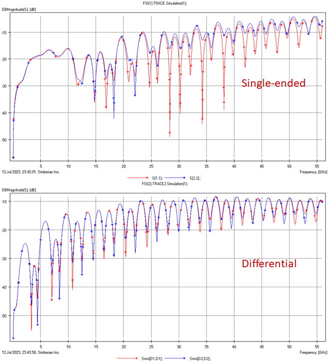
When routing over the 200 mil gap, the results are not so horrible. Although we would typically see return loss anywhere as low as -30 dB or less, we often are willing to accept anything below -10 dB as we get to higher frequencies. Both the single-ended and differential channels meet these criteria up to about 20-25 GHz.
Now we can compare with the case of routing over the 400 mil gap, as shown below.
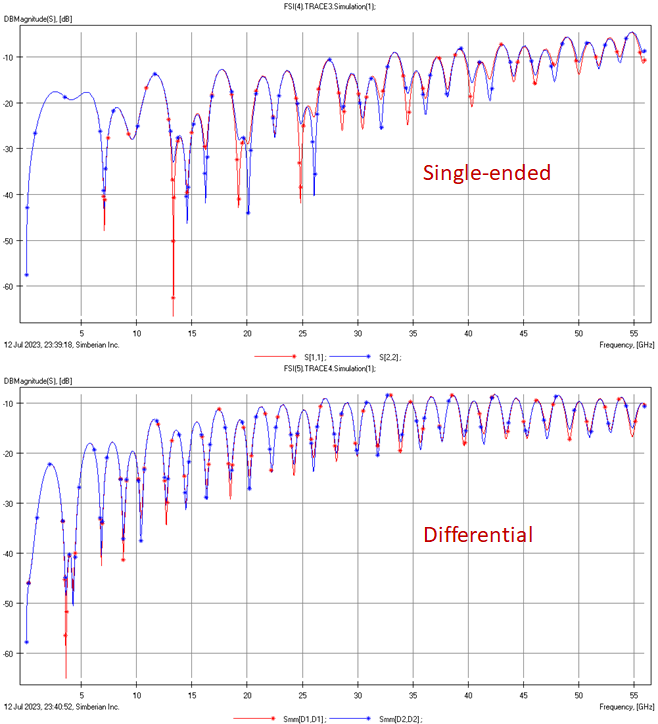
The previous results are already usdesirable, and these are a bit worse as expected. We still see the return loss spectrum approaching the acceptable limit for both the differential and single-ended channels routed over the 400 mil gap. In these channels, we can estimate that the gap adds about 20-25 dB of return loss, depending on frequency, assuming we start from a baseline S11 of -35-40 dB.
Now let's compare to the situation without the gap in the neighboring power plane. This case is shown in the pair of graphs below for the single-ended trace (top) and the differential pair (bottom). Both instances seem to suggest what we would know intuitively just by analyzing the critical length: at low frequencies we still see the decent impedance matching to the reference impedance as we would expect. Note that the S11 and S22 curves are practically identical as we would expect for a uniform transmission line.

A common bandwidth metric that is used to compare S-parameter plots is the -10 dB limit in the return loss spectrum. The table below summarizes the -20 dB bandwidth values extracted from the above set of plots.
The results are quite interesting. Initially the single-ended trace had higher bandwidth, however this could be due to its larger width (8.64 mil for single-ended vs. 6.223 mil for differential) as this would give the single-ended trace lower skin resistance at these frequencies. In both cases, the presence of the gap limits bandwidth by moving the -10 dB frequency point to the left in both cases, just as we would expect. The bandwidth reduction for the differential pair is much smaller because each trace provides a return path for the other trace.

What happens if we route traces in these gaps in the power layer? It should be clear that there will be some crosstalk from the traces in the above layer. Meanwhile, the presence of the power plane and ground plane collectively determine the impedance. You would have both crosstalk and reflections occuring simultaneously, and the amount of each will be more noticeable at higher bandwidths. This supports the points above regarding rise time - striplines carrying slower signals may be fine to route over the gap in a power layer, but faster signals will have their bandwidth overlap with the dip in the return loss spectrum, and the channel may be non-functional.
Summary
In summary, I wouldn’t worry too much about routing traces in the power copper pour if you’re operating with lower-speed digital signals that don’t require impedance control. Just be mindful of the path for electric current around the power plane and try not to cut up the power layer into small islands. In other cases, you should use an additional layer and route there. In addition, be mindful of impedance requirements when necessary: coplanar copper in the power layer that is placed too close to striplines or microstrips will create an impedance deviation, just like with the example I show using coplanar microstrips.
What about any signals adjacent to the power plane? For moderate speed signals, you must make sure there is another nearby reference plane, and avoid routing across the gaps in the power layer. For very fast signals, we quickly see that even with an adjacent ground plane (stripline configuration) does not prevent bandwidth limitation. If your gap in the power layer is larger, then the impedance mismatch will be seen at lower frequencies and will create more reflections that limit channel bandwidth.
The Layer Stack Manager in Altium Designer® can help you specify signal and plane layers in your PCB, as well as define impedance profiles for use in routing. When you’ve finished your design, and you want to release files to your manufacturer, the Altium 365™ platform makes it easy to collaborate and share your projects.
We have only scratched the surface of what’s possible with Altium Designer on Altium 365. Start your free trial of Altium Designer + Altium 365 today.

About Author
Related Resources


Related Technical Documentation


Table of Contents
Take advantage of the world's
most trusted PCB design system.
One interface. One data
model. Endless possibilities.
Effortlessly collaborate with
mechanical designers.
The world's most trusted
PCB design platform
Best in class interactive
routing
View License Options
Thank you, you are now subscribed to updates.