Overview of PCB Workflow Management

Table of Contents
Many industries have a standard engineering process or workflow that they implement to keep everyone on the same page and to ensure teams are productive. Processes and workflows might seem like they eliminate creativity or stifle ingenuity, but they are implemented for many good reasons. In the electronics industry, we implement a specific PCB design flow to guide new products from concept and, eventually, into full-scale production. Electronics engineering teams that work together on new products have to implement PCB workflow management to help them move through the entire design cycle.
How exactly does one manage the workflow of a PCB design team? Individual designers that work on smaller projects should be familiar with the PCB design process and the way in which a new design is moved through each stage. PCB workflow management is implemented on larger teams to help guide a product through each phase and catch any potential errors along the way. To see how PCB workflow management is implemented, keep reading and view some of our related resources.
PCB Workflow Management and the Design Process
Technically speaking. a PCB workflow is nothing more than a process. Several times in other blogs and materials, I have given this definition of a Process. According to the business dictionary:
- A Process is the Sequence of interdependent and linked procedures which, at every stage, consume one or more resources (employee time, energy, machines, money) to convert inputs (data, material, parts, etc.) into outputs. These outputs then serve as inputs for the next stage until a known goal or result is reached.
I have always liked that definition; the inputs being used and modified by a resource to create the output for the input of the next stage, and so on until you reach the desired goal. That is nothing more than a chain. From the very first step to the end, the standard PCB design workflow is a chain of tasks that ultimately produces a set of design outputs that make the product ready to manufacture. The entire job of a PCB designer is to ultimately produce something that will become a physical product.
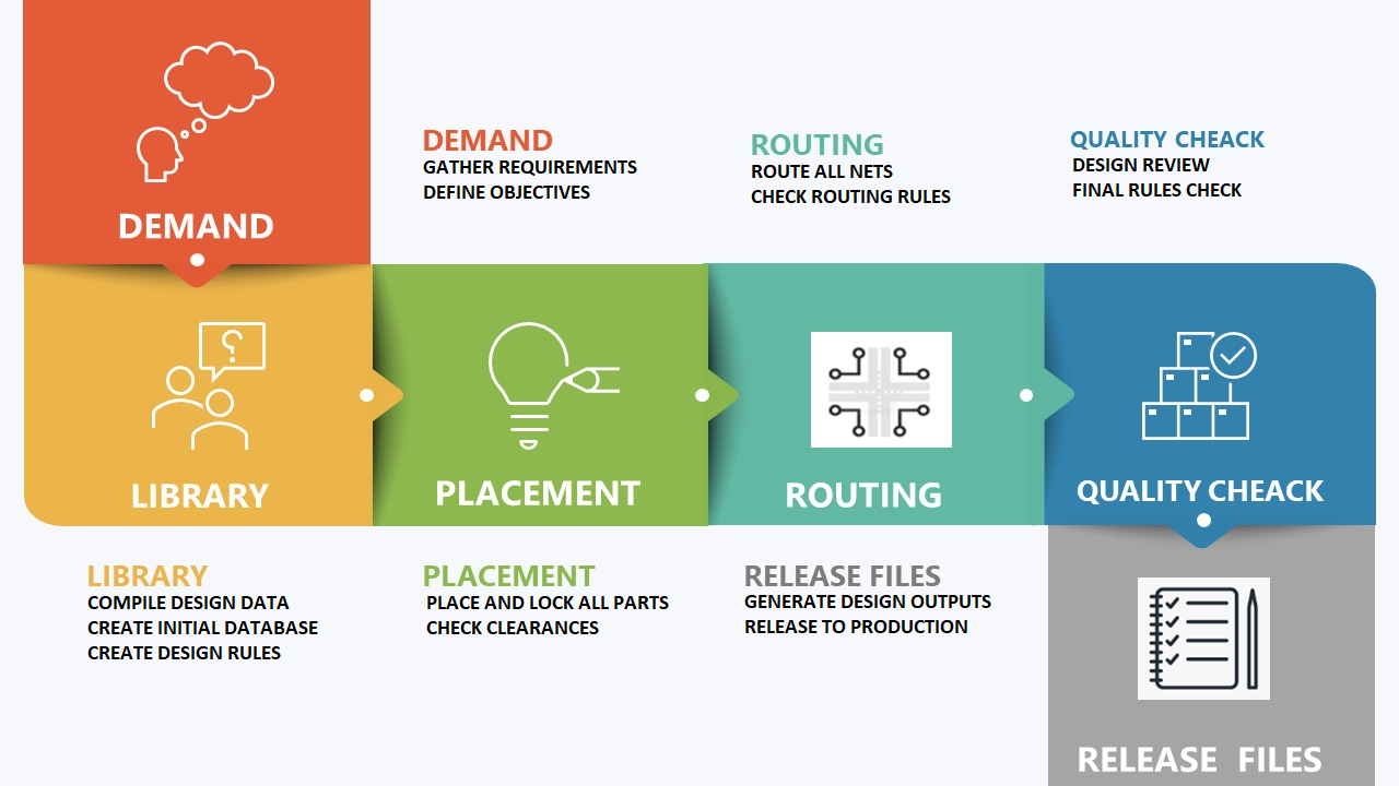
The typical PCB linear workflow is shown in the flowchart below. Although alternative methodologies like Agile flip this to a circular process, the standard PCB design workflow will proceed through all of these steps and ultimately culminate in planning for production.
As we all know, a chain is only as strong as its weakest link, meaning we will need to look at the individual stages involved and determine if there is any possibility for problems. Several things can destroy any process if allowed to go unchecked—but keep in mind that problems are usually a combination of many distinct causes, and when this happens it’s going to require us to do some root cause analysis to determine what the real issues are.
PCB workflow management exists to help design teams move easily through each of these steps while implementing process to address problems along the way. Different products can involve somewhat different workflows as design teams can involve engineers from multiple domains, all collaborating to make a product a reality. PCB workflow processes are often constrained by available design tools and collaboration platforms, but workflow management should still focus on identifying areas of operational improvement to help teams stay competitive.
Assumptions vs. Documentation
The underlying problem with every PCB design issue is that assumptions were made somewhere along the way. Assuming anything is a significant problem. It quickly introduces a high amount of risk to your PCB design.
It is so easy to make assumptions; it usually starts with incomplete information, and because we do not question or verify it, we fill in the blanks with our interpretation of things. Sorry to say we are usually wrong. The more significant problem is that the assumptions are taken to be correct and not verified in any way. So they continue down the design workflow process until it gets fabricated into a design, and the board ends up as scrap.
The best way to avoid the need to make assumptions and ensure design errors are caught early is through comprehensive documentation. On the front-end, product functional requirements must be gathered to ensure the remaining design tasks and manufacturing needs are fully understood.
Throughout the design process, and important aspect of workflow management is visibility into who changed which aspects of a design. The ability to access and compare changes throughout the design process keeps teams honest and helps ensure products can be brought to market without underlying problems. Documentation will be used throughout a product's lifecycle to ensure a product can remain competitive for the longest possible time, and possibly refreshed later with new features and technology.
Tasks vs. Milestones vs. Deliverables
Because the PCB design workflow is a chain, we must look at each link or stage of the process. In a specific stage, we have an input, then a resource of some kind has its necessary tasks, and that stage has set deliverables or outputs. These outputs are the inputs for the next stage, and finally, a verification or milestone process is conducted. PCB workflow management focuses on moving through the tasks, milestones, and deliverables for each stage.
For example, schematic capture is one of the front-end engineering stages in the PCB design process. It just happens that the inputs for this stage are the components from your libraries:
- Tasks: Place components, wire them up, make your off-page connections to other sheets, etc.
- Milestone (Verification): Running of the ERC and Connectivity Rules.
- Deliverables: Completed Netlist that gets pushed into the PCB stage.
A fortunate aspect of the PCB Design process is that it can be described as cookie cutting. The same Tasks, Milestones, and deliverables are very consistent between designs. Project managers, engineering managers, and stakeholders need the ability to see, trigger, and review each of these aspects of the PCB design workflow, and they need a singular platform to do it.
The Best Tools for PCB Workflow Management
With so much to manage in the standard PCB workflow management process, even for relatively simple products, engineering teams need a complete product management suite that unifies designers and engineers across domains. The Altium enterprise solutions provide the industry's newest workflow management platform dedicated solely to PCB design and production. Within a unified platform, Altium enables the last mile of digital transformation that unifies design teams, design data, and design processes for all product stakeholders.
In addition to the standard set of PCB design tasks involved in engineering a product and creating a physical layout, the Altium enterprise solutions provide multiple PCB workflow management capabilities within a unified design workflow.
- Unifying resources - PCB design teams can unify their design and management resources in a single design environment. It does more than keep all your design data in one place; users can establish traceability and interactivity, monitor project and product status, and manage all project activities in a single platform. Learn more about project management in hardware development.
- Cross-domain collaboration - Electrical engineers and PCB layout designers can work efficiently on cross-functional teams with visibility into different design domains. Adjacent design domain integration includes MCAD users, procurement teams, manufacturers, and much more. Learn more about ECAD integration.
- Product lifecycle management - Altium enterprise solutions provide the same type of integration and product lifecycle tracking found in Altium 365, but with additional management features that fit within multifunctional team workflows. Learn more about PLM integration.

Access projects and manage workflows.
In the past, engineers would have to work with multiple applications and file sets to implement these workflow management capabilities. The Altium enterprise solutions provide a customizable workflow management solution designed for enterprise-level users. Users can give all stakeholders the visibility they need for successful PCB workflow management and transition from design to manufacturing, release to market, and beyond.
Conclusion
Although design and engineering workflows can be complex, and they often involve orchestrating multiple parties, it is possible to streamline the entire process when product data is aggregated into a single platform. Enterprises need to move their designs from concept to production while enabling collaboration across design teams. Now it's possible to implement these important management tasks in a single platform to ensure your engineering team can seamlessly transition from concept to full-scale production.
When you're ready to revolutionize PCB workflow management for your design team, use the powerful set of PCB design features and workflow management features in the Altium enterprise solutions. They build on top of the existing PCB design features in Altium Designer® to include workflow management tools demanded by enterprise customers. All project stakeholders can operate within a single platform and implement comprehensive workflow management system that helps guide innovative products to market.

About Author
Related Resources

Related Technical Documentation


Take advantage of the world's
most trusted PCB design system.
One interface. One data
model. Endless possibilities.
Effortlessly collaborate with
mechanical designers.
The world's most trusted
PCB design platform
Best in class interactive
routing
View License Options
Thank you, you are now subscribed to updates.