What is Hybrid Beamforming?

Beamforming is an important broadcast method that involves use of antenna arrays in a wireless system to transmit electromagnetic energy along a specific direction. More wireless systems are expanding their ability to handle multiple users (or targets) with beamforming and MIMO. This is already used in radar, WiFi, and in newer high-bandwidth communication systems (5G). For the systems designer, it is important to understand the layout requirements for the antenna arrays in these systems, which are related to the beamforming methods used in RF systems.
When it comes to beamforming, there can be some confusion as to any distinction from MIMO, and the two are sometimes stated as being unrelated to each other. This is only true in a special case, but in general multi-user MIMO (MU-MIMO) requires beamforming to direct a modulated signal to multiple targets.
In this article, we’ll look at beamforming implementation in an advanced method combining analog and digital techniques, known as hybrid beamforming. This method blends both digital and analog techniques to create multiple beams and thus reach multiple users with varying intensities. In the case of an RF imaging system or a radar system, hybrid beamforming in a MIMO technique also allows tracking of multiple targets with adjustable resolution.
Hybrid Beamforming Overview
Before looking at the system design methodology for hybrid beamforming, I think a short overview of analog and digital beamforming methods is important. Beamforming is a technique for engineering the emission distribution from an antenna such that electromagnetic energy is directed along a specific path or angle.
The key structure needed to perform beamforming is an antenna array, or a regularly spaced group of antennas in two dimensions. By controlling the relative phases and amplitudes of the signals sent to the phased array, you can control the direction of the emitted beam. The number of possible beams that can be emitted can be further doubled by exploiting polarization, or by only emitting electromagnetic radiation along one direction from each emitter in the array.

Analog Beamforming
Analog beamforming operates by sending a signal to multiple antennas in an antenna array. The signals sent to each antenna are delayed by a specific time window, which applies a phase difference to the emission emitted from each antenna in the array. These antenna arrays are better known as phased arrays, and this application of phase difference has historically been the dominant method for beamforming in RF systems.
In this method, we input a single signal (possibly modulated) into the antenna array; this signal is phase shifted by a transceiver before reaching each antenna. The spacing between antennas will determine the beam direction and the intensity of sidelobes. The ideal gain increase will be log(N), where N is the number of antennas in the array. Finally, the intensity distribution along one dimension (shown below) is a case of diffraction from multiple emitters.
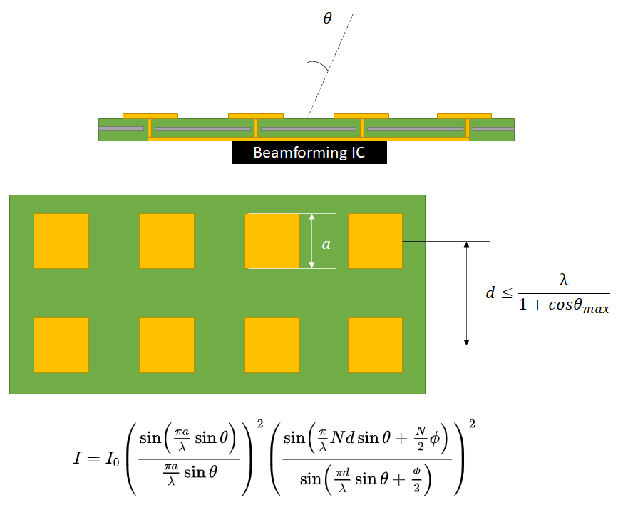
These arrays can be scanned by adjusting the phases. For the 2D array, you can design the field of view such that the maximum scanning angle in the vertical direction depends on the following factors:
- The emission wavelength (in free space)
- The size of the radiating element (vertical size in the above example)
- The distance between radiating elements (vertical distance in the above example)
The same idea applies in the horizontal direction. You would now have two orthogonal scan directions, and these can have different resolutions depending on the size, number, and density of radiating antenna elements. I’ll look at this much deeper in an upcoming article as it is an important topic in a few important areas of RF design.
Digital Beamforming
Digital beamforming takes a different approach and is much less intuitive. In digital beamforming, multiple modulated signals are sent to the antenna array, and the phases and amplitudes of the signals sent to the array are combined to produce the desired beam pattern. The most basic case uses a single input data stream (such as QAM constellation points) sent to multiple antennas, and the amplitudes are combined to produce the desired emission pattern.
Digital beamforming is actually a special case of a more advanced type of broadcasting called precoding. The beam pattern can be defined as a sum of products of a carrier wave and a spatial distribution function (Y). The relationship between the emitted signal from each element (y) and the input signal to each element (x) is defined in a precoding matrix as shown below:

The key here is to determine the precoding matrix defined above. This involves working backwards from the desired emission pattern (the set of y functions) and solving a system of equations for the N radiating elements. This can be done in software or in a system controller (FPGA). The emission can then produce multiple beams from the same array in different directions and/or in different time windows.
The time windowing issue (essentially time-division multiplexing) is not appropriate for something like 5G with MU-MIMO, where orthogonal frequency-division multiplexing (OFDM) is used to allow broadcasting of independently modulated orthogonal subcarriers. In addition, beamforming is used to enable spatial multiplexing within the array, which is essential for reaching multiple users.
Hybrid (Digital + Analog) Beamforming
Now I think we can look closer at hybrid beamforming. In hybrid beamforming, we’re combining digital beamforming with analog beamforming using subarrays. First, let’s think about how this works with a set of input data streams (x).
- The set of input data streams is first precoded as in digital beamforming.
- Instead of outputting the stream directly to the entire array, the precoded streams are sent to individual analog beamformers, or sub-arrays.
- The stream sent to each sub-array is then phase shifted to produce a beam only from that sub-array, which is directed at the end user.
This follows the description outlined in the block diagram below.

From the above image, I hope it is clear what is happening at each antenna. The antennas are using precoding to define a superposition among multiple beams for several data streams in order to achieve spatial multiplexing. As long as all elements in the precoding matrix are non-zero and complex, then all signals are sent to all antennas, but with mixed amplitude/phase combinations for each input stream. The result is the desired beamforming for each input data stream.
This is how you can get higher throughput with an RF system that must broadcast to multiple targets; you can broadcast at multiple orthogonal carriers in the same time window while using beamforming to enforce spatial multiplexing. With something like mmWave sensing, you can then broadcast multiple beams and track multiple targets, or you can simply build an extremely dense point cloud without the complications of an optical system like lidar.
Where Is Everything Placed on a PCB?
At some point, the antennas in the array will need to be placed on a PCB and connected to the system controller/transceivers.
In terms of the structure in a PCB layout, you might think that you must have to separate each analog sub-array into a different region of the PCB. That is not necessarily the case, but doing it in this way could make placement and routing much easier. This is because the analog beamformer control unit has to set a definite phase between only the antennas in the sub-array, rather than between all antennas everywhere. It is also difficult to co-locate all the transceivers and the digital controllers; spacing them out into different sub-arrays is much easier.
To see what I mean, take a look at the image below with a purely analog system. A system oscillator is needed to synchronize all transceiver elements in the system, and each transceiver can then apply the required phase across its own section of the array. The problem comes in the need to apply length tuning across all transceiver elements.

Eventually, this requires excessive layer counts with controlled impedance to reach every transceiver while maintaining the timing phase across the system. As the array scales, you may need to place the control chips on the backside, which will require the feedlines be brought into the antennas with vias.
With a hybrid beamforming approach, the main system controller is synchronizing across multiple ADC/DAC + PA elements with a fast digital interface and an embedded clock (such as JESD204C). This means you will have reduced dependence on synchronizing an RF oscillator across your entire system as this will only be required within the subarrays.

Aside from these placement and routing points, make sure to follow some of the standard RF PCB design best practices for stackup design, transmission line design, and via design. The point about via design is very important because placing all the antennas can take up a ton of space, so transceivers might need to be placed on the back side of the board with digital routing on internal layers.
- Learn the fundamentals of hybrid RF PCB stackup design
- Learn more about high-frequency transmission line design
- Learn more about signal chain design for RF systems
Final Thoughts
Analog beamforming can quickly become unscalable when applied over large arrays. For smaller footprint MIMO systems, possibly with multiple transceivers, the system-level synchronization that needs to be enforced in analog beamforming can be very difficult. The issue is the need to span the system’s main oscillator across the transceiver elements so that emission from the array is synchronized everywhere.
You might be thinking “hey, I don’t design 5G base station equipment, so why do I need to know this?” These techniques with beamforming go beyond 5G and are used in other important application areas:
- Phased array radars
- New mmWave sensing systems, specifically in ADAS
- Ultrasound imaging
- IEEE 802.11 standards (specifically WiFi 5 and later)
- Sonar
Phased array designs rely on more than just antennas. You’ll have to understand where to place and route signals to ensure phases and amplitudes from emitters have the values you intend across the entire array. For electromagnetics applications, phased array antennas can be easily placed in a PCB layout as polygons, but be mindful of the placement and routing challenges outlined above.
When you need to place antennas, route feedlines, and design your system for hybrid beamforming, use the complete set of PCB design tools in Altium Designer®. When you’ve finished your design, and you want to release files to your manufacturer, the Altium 365™ platform makes it easy to collaborate and share your projects.
We have only scratched the surface of what’s possible with Altium Designer on Altium 365. Start your free trial of Altium Designer + Altium 365 today.

About Author
Related Resources


Related Technical Documentation


Table of Contents
Take advantage of the world's
most trusted PCB design system.
One interface. One data
model. Endless possibilities.
Effortlessly collaborate with
mechanical designers.
The world's most trusted
PCB design platform
Best in class interactive
routing
View License Options
Thank you, you are now subscribed to updates.