What's In Your BGA Land Pattern and Footprint

Table of Contents
If you look in datasheets for most components, you’ll often find a recommended land pattern, usually alongside some mechanical package information and assembly information. This is not always the case with BGA components, especially components with high ball count. There are a few reasons for this that we can speculate: those ball counts might just be too big to put into a single page, or the manufacturer just expects you to know how to create that land pattern. Sometimes, the recommended land pattern for the manufacturer’s BGA package is in a separate document, but you wouldn’t know this unless you did some digging.
If you’re in a situation where you can’t find a footprint for your BGA, and you can’t find a recommended land pattern, then we have some simple guidelines you can follow to help ensure accurate assembly. There is an IPC standard you can follow that will help you create your land patterns, or you can use an automated footprint generator to create your land patterns if you have the right PCB design software.
BGA Land Pattern Creation
All PCB footprints need a land pattern to define the location of pads. In addition to the pad size and location, there is solder mask expansion to consider, as well as whether to use an SMD or NSMD pad. For any BGA component, there are four important parameters that determine how you will create the land pattern for the component:
- Landing pad diameter
- Pad pitch
- Ball size on the component
- Allowed/required solder mask expansion (SMD or NSMD)
The pad pitch and the ball size will determine the approach you take to create the BGA land pattern for your footprint. Specifically, these will determine the pad size you should put into the land pattern. The pitch will then determine whether you should use SMD or NSMD pads in the land pattern. This is all a delicate balance that is primarily driven by the package and assembly constraints, but there is a simple set of guidelines that can help you create an accurate land pattern for your BGA.
IPC-7351 Standard
The IPC-7351 standard provides guidelines on land pattern creation for standard component packages that will help ensure high yield in standard assembly processes. These guidelines are a good place to start creating your BGA land pattern for your components. The pad size depends on the ball size on the BGA package, as shown below.
|
|
|
|
|
|
|
|
|
|
|
|
|
|
|
|
|
|
|
|
|
|
|
|
|
|
|
|
|
|
|
|
|
|
|
|
|
|
|
|
|
|
|
|
|
|
|
|
|
|
|
|
|
|
|
|
|
|
|
|
|
|
|
|
|
|
|
|
|
|
|
|
|
|
|
|
|
|
|
|
|
|
|
|
SMD or NSMD?
For larger ball pitches (between 0.5 mm to 1 mm), you will likely be just fine using either an NSMD pad or SMD pad in your land pattern. There will still be sufficient solderable area on the pads to provide adhesion. The larger pad area used for these BGAs will also prevent the pad from peeling off of the surface layer if the solder process runs too hot. If your pitch is closer to 1 mm, you could set 0 mil solder mask expansion and allow the fabricator to expand it based on their judgment. Even if expansion is left at 0 mil, misregistration will be small enough that you won’t significantly reduce the solderable area.
At 0.5 mm and smaller pitch values, the pad should be placed as an SMD pad. The reason is that smaller pads are more likely to peel if they get too hot. Also, the solder mask around the pad creates a dam that holds the molten solder ball in place during reflow. Set a larger pad size and use a negative solder mask expansion to set the visible solderable area on the pad.
Speed Up BGA Land Pattern Creation
Today, there are several resources where you can find footprints for your BGA components. Based on pitch and ball sizes, it’s even possible to take an existing BGA footprint with higher ball count than you need, and then modify this so it can be used with your desired BGA component. If you’re an Altium user, you might be able to find your BGA footprint in the Manufacturer Part Search panel.
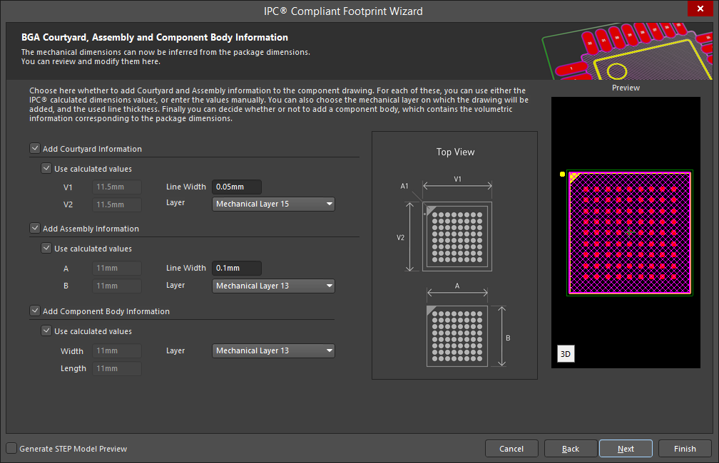
If you’re working with a less common component or a proprietary component, you can use a footprint generator in your PCB design software. The IPC-Compliant Footprint Wizard helps you quickly create a high ball count footprint without forcing you to manually arrange pads in the footprint. You can set important land pattern characteristics like solder mask expansion, pad size, pad pitch, and package size in this tool by configuring a few settings. Some land patterns omit some pads/balls, even in high ball count BGAs. Once you generate a standard BGA land pattern for your component, you can modify this by adding/removing any of the pads.
Although you might not need to create your own footprint for every component, the guidelines above can be used to check footprints that you receive from an external source. Unfortunately, there are no standard PCB design rules that incorporate these guidelines, so you have to address these through manual inspection, or you need to create a component class for fine-pitch components that applies the required solder mask expansion and clearance rules. In my opinion, you should look at the fine-pitch BGAs individually when checking footprints.
If you want to make sure your BGA land pattern enables accurate assembly, use the IPC Compliant Footprint Wizard in Altium Designer®. It’s easy to generate footprints for standard component packages while remaining compliant with IPC standards in this utility. Once you’ve created your PCB footprints and you want to share them with your collaborators, your team can work together through the Altium 365™ platform. Everything you need to design and produce advanced electronics can be found in one software package.
We have only scratched the surface of what is possible to do with Altium Designer on Altium 365. Start your free trial of Altium Designer + Altium 365 today.

About Author
Related Resources


Related Technical Documentation


Take advantage of the world's
most trusted PCB design system.
One interface. One data
model. Endless possibilities.
Effortlessly collaborate with
mechanical designers.
The world's most trusted
PCB design platform
Best in class interactive
routing
View License Options
Thank you, you are now subscribed to updates.