When to Use Tented Vias in Your PCB Layout

There are some guidelines I see many designers implement as a standard practice, often without thinking about it. Some of these practices are misunderstood or implemented without best practices, such as copper pour in signal layers. Others are implemented without thinking about the potential problems, but only because those problems arise in corner cases. One of these is the use of tented vias, which is sometimes implemented in a PCB layout by default.
Is this always the right practice? And what are the possible reliability concerns with tented vias? These are important questions, especially when reliability concerns get brought up in regard to high aspect ratio vias and stacked microvias. In this article, we’ll examine some of these design points surrounding via tenting and when you should avoid using it in your PCB layout.
When to Use Tented Vias
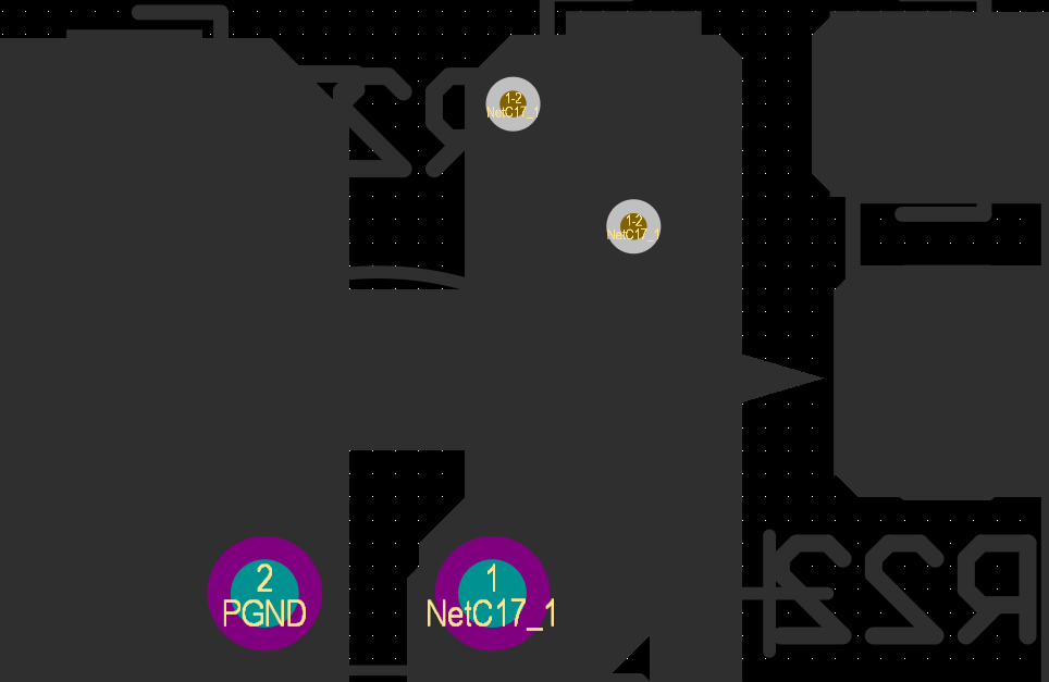
The idea behind via tenting is simple: you’re covering any vias in your PCB with solder mask so that any pad/ring on the via hole, and the via barrel itself, are not exposed to the environment. The solder resist is placed to provide some measure of protection for the via pad and the plating inside the via barrel. If you look at a PCB layout, you can spot tented vias just by looking at your solder stop mask layer; the same applies to the Gerber file for that solder mask layer.
Tenting of vias is sometimes seen as a DFA requirement, as well as a reliability requirement. Some of the stated benefits and drawbacks of via tenting include:
- Tenting prevents exposure to environmental factors that reduce device lifetime, such as noxious chemicals or humidity.
- Tenting costs less than via plugging or filling/plating with an epoxy, making the simplest process you can use to protect vias.
- Tenting can both aid and interfere with assembly, depending on the particular component being placed and soldered on the board.
Let’s look at each of these areas to see some instances where we might need to include or omit tented vias.
Preventing Solder Wicking
Vias placed close to SMD components may provide a path for solder wicking onto the back side of the board. There are three possible ways to solve this:
- Reduce the paste mask opening so that less solder paste is applied to the SMD pads in question
- Move those vias farther away from SMD pads, and ensure there is some solder mask dam between any pad and its connecting via
- Tent any vias near SMD pads selectively without modifying the paste mask
In my opinion, #3 is the best option given all other possible choices. The reason for this is that it is a very simple change that only requires closing the solder mask expansion on specific vias.
Environmental Protection for Small Vias
Tenting is best used on small vias with a finished hole diameter of less than about 12 mil. The specific diameter limit depends on the LPI solder mask solution, and your fabricator should be able to recommend a maximum via diameter to ensure reliable tenting. If the via diameter is too large, the solder resist could break and leave a small hole, which would allow contaminants into the via barrel. This is where reliability concerns arise, particularly when environmental protection is needed.
When the interior of a via is exposed to the environment and it is not protected with a plating finish or other material (e.g., conformal coating), then the exposed copper could slowly corrode. The process speeds up if the via is only tented on one side and some contaminant could pool inside the via barrel. This exposure might also cause the device to fail early. Therefore, any device that might be exposed to an environment where a contaminant could pool inside the via barrel should have tenting applied where possible.

In the case where you leave some of the vias untented, you can always coat the PCBA in a conformal coating to give it that additional level of environmental protection. This would be a great solution if the environmental concern was something like humidity or dust, but it might be problematic with outgassing in a low pressure environment, such as in space or in a specialty industrial system.
Assembly Concerns
Tented vias can create some assembly concerns in certain cases. The potential assembly problems depend on whether you need to assemble a fine-pitch component, or you’re working at high densities that bring you close to the limit where via in pad might be needed. Tenting vias in PCB assembly should be considered from two perspectives:
- Is there a chance the solder will wick onto the back of the board during assembly? If yes, then tent the vias near the component footprint.
- Will excessive flux residue cause problems with contamination and possibly shorting? If yes, then un-tent the vias near or under the component footprint.
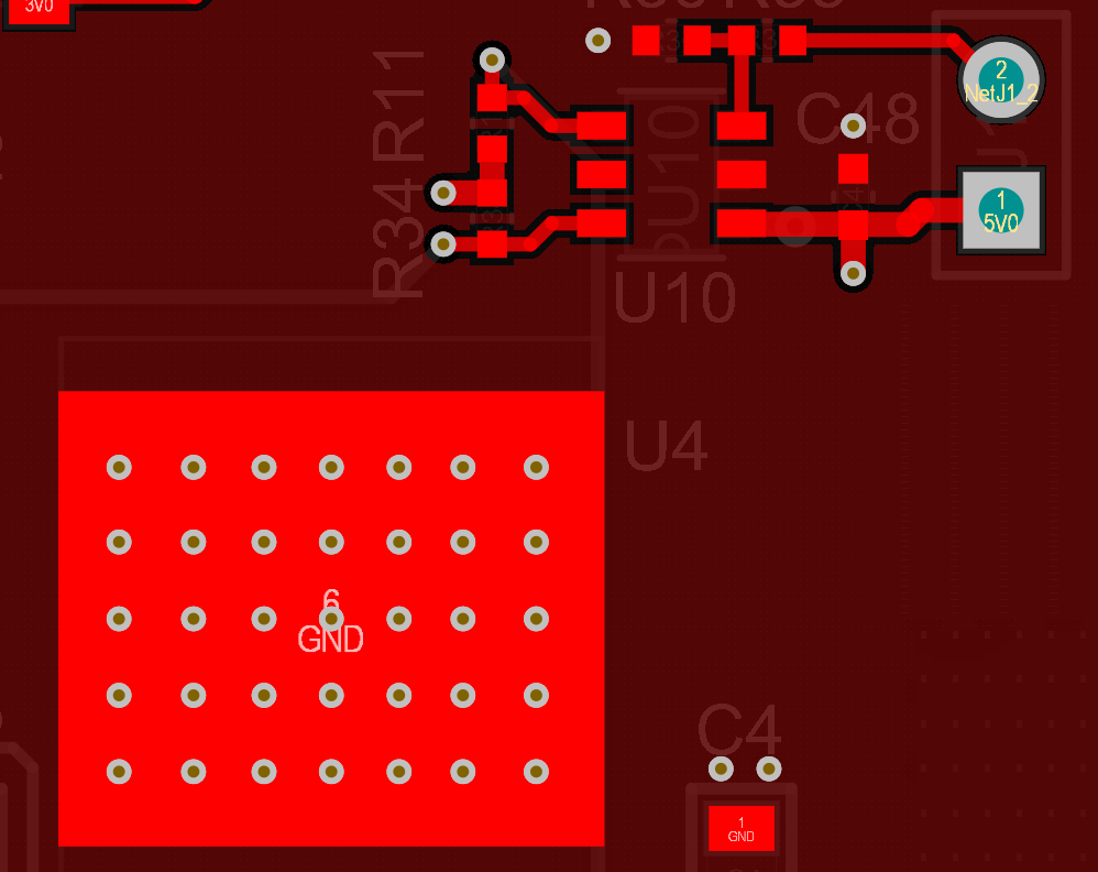
A great example here is a ground pad underneath a QFN component or large TO package. This pad will contain vias, but it needs to be soldered to the component to make an electrical connection and to ensure heat easily transfers away from the component. However, the back side of the board might have tenting applied to prevent solder wicking. I would argue that, in this case, wicking is more important and those vias should be tented, especially if there are other components on the back side that might short if any solder wicking occurs.
For a BGA with a dog bone fanout, it should be clear that the two objectives are in conflict. If you leave vias in the fanout untented, you’ll have a clear escape route for flux during assembly, and the surface plating material will protect the copper from environmental damage. However, if you tent these vias, on the same side as the BGA pads, you will prevent solder from wicking into the back side of the board.
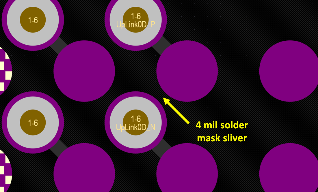
In my opinion and experience, the dividing line is the allowed solder resist sliver between the BGA pad and the via. If you leave the vias untented and the solder stop mask sliver is too thin, it can break off after fabrication, meaning you lose your solder mask dam and there is a risk the BGA solder ball will flow through the open via barrel. If the untented via would leave behind a solder mask sliver that was too thin, I would recommend tenting the vias and request a reliable no-clean flux is used during assembly. The assembler should know or have data as to whether their no-clean flux will ever cause the solder balls to short during reflow.
One Side or Both Sides?
The not-so-obvious next question to ask is: should you tent on one side or both sides?
My view is, if you’re going to tent vias, then do it on both sides. The exception is with via-in-pad, vias in an exposed copper polygon/rail, or vias in a ground pad (see the TO package example below). These features require exposed copper, thus the via will be exposed on one side and you will only be able to tent on the other side. Otherwise, once vias become large enough, leave them untented and select an appropriate plating that will protect the exposed conductors.
Summary
Obviously, from the list of possible concerns above, there is a tradeoff between tenting to protect against potential environmental contamination, and leaving a design untented to ensure assembly contaminants can exhaust themselves from the assembly. If either of these are a concern in a particular system, then the PCBA should be thoroughly tested to ensure it will operate correctly and that the design will not suffer from reliability problems based on tented vias.
When you need to select and assign tented vias in your PCB layout, use the complete set of easy-to-use CAD tools in Altium Designer®. Once your design is ready for a thorough design review and manufacturing, your team can share and collaborate in real time through the Altium 365™ platform. Design teams can use Altium 365 to share manufacturing data and test results, and design changes can be shared through a secure cloud platform and in Altium Designer.
We have only scratched the surface of what’s possible with Altium Designer on Altium 365. Start your free trial of Altium Designer + Altium 365 today.

About Author
Related Resources


Related Technical Documentation


Table of Contents
Take advantage of the world's
most trusted PCB design system.
One interface. One data
model. Endless possibilities.
Effortlessly collaborate with
mechanical designers.
The world's most trusted
PCB design platform
Best in class interactive
routing
View License Options
Thank you, you are now subscribed to updates.