5G Antenna Tuning in Mobile and IoT Devices
Table of Contents

5G antenna tuning is like tuning a guitar as you play
Guitar players know all about tuning their instruments. Whether swinging a whammy bar on stage or just ensuring each string hits the right note, this tuning changes that the resonant frequencies of each to the tone desired by the musician.
To continue the recent series of articles on PCB design for 5G systems, one other aspect of designing RF design for 5G-capable wireless systems involves a technique called antenna tuning. This technique is required in 5G systems that operate beyond WiFi frequencies in order to keep power consumption low, provide the bandwidth required for carrier aggregation.
Carrier aggregation and multiple input multiple output (MIMO) require multiple antennas that operate simultaneously. 5G also mandates four independent downlink channels for most bands, meaning new mobile devices require four antennas for cellular communication. Note that this does not account for other capabilities like NFC. Antenna tuning techniques allow antenna resonant frequencies to match particular 5G bands simultaneously in order to maximize antenna efficiencies/minimize return loss in the required bands.
5G Antenna Tuning Switches
In 5G wireless systems, carrier aggregation delivers higher data rates with increased bandwidth by combining at least two carriers with mmWave frequencies, typically in different frequency bands. The number of available bands is much larger than the number antennas in a smartphone or other mobile devices, thus the resonances in an antenna must be actively tuned during operation in order to operate in multiple channels simultaneously.
Antenna tuning is also important for compensating changes in the resonance frequency when a mobile device is held in the user’s hand or brought up to the head. This causes a redshift in the resonant frequencies, thus the scattering parameters shift to lower frequencies. Antenna tuning can be used to adjust the resonance frequencies back to the intended frequencies.
There are two methods used to tune an antenna during operation: impedance tuning and aperture tuning. Both methods require the use of an antenna switch to change the resonance frequencies of an antenna. Antenna switches are commercially available as surface-mount ICs. Aperture tuning ICs typically include enough supporting electronics such that external bypassing and filtering is not necessary, while impedance tuning ICs typically require some external passives for bypassing and filtering.
Typical switch connections for impedance tuning and aperture tuning
Aperture Tuning
Aperture tuning allows a system with an antenna to switch between frequencies in two ways. First, an individual resonance can be tuned capacitively or inductively; the aperture switch plus the antenna acts like an equivalent RLC circuit, which modifies the natural frequencies of the antenna. Signals received by the antenna can then be demultiplexed into individual channels and digital data can be extracted in parallel.
Placing tuning switches at multiple locations along the length of a single antenna allows a single antenna to support a wide range of frequency bands that correspond to different natural resonances of the antenna. Each of these resonant frequencies can be tuned independently by routing the tuning switch connection close to the apex of the voltage distribution for that frequency. This allows different resonances to be turned on and off as desired. When one switch is placed close to the node for one resonant frequency but near the antinode of a second frequency, the first frequency can be tuned without significantly impacting the second frequency.
Each feed line from a tuning switch routes to its particular location on the antenna using a via. An antenna tuning switch IC can be placed behind the ground plane on the antenna module, although it is recommended that sufficient clearance from the antenna ground plane be used to avoid parasitic capacitive coupling with the antenna switch.
Impedance Tuning
Impedance tuning is normally used with frequency-division duplexing (FDD) in order to broaden the bandwidth of an antenna within a particular range so that it can receive/transmit with uniform insertion/return losses at multiple frequencies. The downside is that broadening the bandwidth for use with FDD allows unwanted frequencies to be received by the antenna with high efficiency, and the unwanted signals will have to be removed via active filtration before or after multiplexing. This is where a tuning algorithm implemented with a MCU, CPLD, or other programmable device can be very valuable as it allows very accurate tuning and filtration.
Another way to think of impedance tuning is that the tuning switch changes the impedance of the antenna at a particular frequency, thus the name. This compensates for impedance mismatch loss at particular frequencies in the event of a frequency shift. This requires careful impedance controlled routing along the feed line and calculation of the antenna’s impedance at the desired frequencies in order to provide the right level of compensation.
Just like an aperture tuning switch, an impedance tuning switch and the antenna form an equivalent RLC circuit. Since an impedance tuning switch appears as part of the feed line, it does not require any extra vias to connect to the antenna. However, proper clearance should be maintained from the antenna’s ground plane in order to avoid parasitic capacitive coupling.
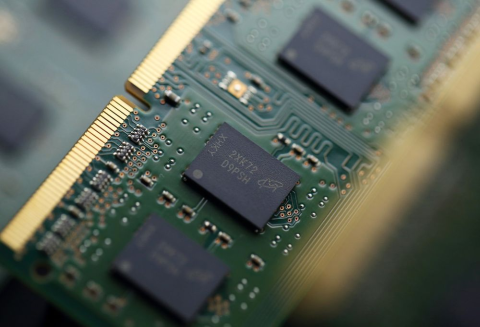
PCB for a smartphone
5G antenna tuning techniques form the foundation of wireless communication with new mobile and IoT devices, and PCB designers are going to need design software that allows them to incorporate off-the-shelf or proprietary ICs. A PCB design software package like Altium Designer gives you CAD tools for antenna design and PCB layout features that are adaptable to any application. Altium Designer’s suite of simulation tools also helps you verify high speed, high frequency, and mixed signal designs.
If you’re interested in learning more about Altium Designer, you can contact us or download a free trial and get access to the industry’s best layout, routing, and simulation tools. Talk to an Altium expert today to learn more.

About Author
Related Resources


Related Technical Documentation


Take advantage of the world's
most trusted PCB design system.
One interface. One data
model. Endless possibilities.
Effortlessly collaborate with
mechanical designers.
The world's most trusted
PCB design platform
Best in class interactive
routing
View License Options
Thank you, you are now subscribed to updates.