Communicating PCB Layer Stackup Needs to Manufacturers

Table of Contents
In the business of PCB design, communicating needs to manufacturers and vendors is a top priority. The context of our requests is sometimes lost either by not providing the correct information, not listing enough information, or not giving any information. Although the experienced PCB designer can take steps to specify everything they want to see in their PCB stackup, eventaully the manufacturer will handle that decision in an effort to balance available materials with processing capabilities and yield.
Stackups describe more than the basic construction of the PCB; built into the stackup are many other design considerations defined by the material properties of your core and dielectric materials. To ensure your design is compatible with your fabricator's capabilities, material stocks, and impedance requirements, designers have to make sure their stackup requirements are clearly defined. If you follow my advice when initially creating the design, and you initially ask your fabricator what stackups they have available, then you'll be in good shape. If you design around that layer stack, then working with your fabricator will be much easier.
What if you have an existing design, and you need to get it produced anywhere with compatible material sets? How can you reduce the risk that the board you receive does not hit your requirements? That's what we'll look at in this article. If you follow some of these tips, you'll be designing WITH manufacturing, not just designing FOR manufacturing.
Ensure PCB Layer Stackup Needs Are Specified
As I mentioned above, on the initial iteration of a design, it's typically the case that you can obtain a standard stackup and use that in your design. This is the fastest way to get your prototype designed and put into production. The other option is to at least design your own stackup with materials you select, and then qualify this with your fabrication house. They'll tell you whether or not they can produce it, and you can decide how to proceed from there (either redesign the stackup, or send it somewhere else).
When the design is already finishsed, it's a bit of a different story. When you go to produce the design, you have to ensure the bare board fabricator can hit multiple specifications, including:
- Layer characteristics - This includes layer thicknesses, copper weight, copper foil type (reverse treated, electrodeposited, rolled copper, additive, etc.), and laminate construction/weave style.
- Dielectric and impedance requirements - If you have an impedance specification (both for signals and power) you need to hit, then you need to specify the dielectric constant in your layers along with layer thicknesses and copper.
- Allowed substitutions and tolerances - This is where your fabricator can see what you've given them permission to modify in order to ensure the design can be reliably produced anywhere.
We don't often talk about Point #3 and instead focus of DFM as part of Points #1 and #2. If you can account for possible changes needed in your PCB layer stackup in Point #3, you can eliminate the risk that you receive boards that don't hit your specs.
Just to ensure your PCB stackup needs are met, you have an important document you can use to specify your circuit board requirements: your PCB fabrication drawing. You'll want to use both a stackup drawing and your fabrication notes to communicate your PCB layer stackup requirements to your manufacturer.
Start With a PCB Layer Stackup Drawing or Table
Inside your fabrication drawing, you can immediately specify most of the requirements for your stackup with a layer stackup drawing. This is the simplest way to give your fabrication house the basic requirements you want to see in your board. The example below is a design for a 4-layer board that could be used for a high speed PCB, power regulator module, microcontroller board, or another general-purpose board.

From this drawing, we can already see several important specifications that your fabrication house will need to meet:
- Layer thickness and count
- Copper weight on each layer
- Specific material set (ITEQ IT-180BS/IT-180C in this case)
- Gerber file extension matching each layer
Sometimes, when I receive requirements lists from clients, these points will be compiled into a stackup document. When submitting your design outputs to your manufacturer, it's fine to include a stackup document or other requirements document as part of the file package, but this information should also be reflected in a fabrication drawing. The best way to do this is with a stackup drawing as shown above.
What about impedance and dielectric properties? If you're designing with a specific material set in mind, then you don't need to list these explicitly, although these can be included in your PCB layer stackup drawing. To ensure your fabrication house is accounting for these tolerances in your design, you will have to specify acceptable tolerances on trace widths and layer thicknesses.
Tolerances in Your Stackup and Trace Widths
To ensure you hit a dielectric constant target, thermal/chemical property target, or an impedance target (assuming you've specified this), there are three ways to proceed in your design:
- Before doing any design work, get your stackup approved by your fabrication house. If they approve it, make sure they specify a trace width for your impedance value based on controlled impedance data. If you design around this trace width and layer stack, then you'll know the specifications you provide in your fabrication drawing will produce the desired electrical behavior.
- Specify the IPC slash sheet conformance for any compatible materials that will be used in the PCB stackup. You need to know a desired slash sheet for an initial material selection.
- Allow the fabricator to adjust trace widths as needed in order to accommodate any material swap used in the PCB stackup. You don' need to specify a specific slash sheet or material name, although you're free to do so in your fabrication notes.
Option #1 ensures your board will be accurate, but only at fabricators that offer only your specific material set. Options #2 and #3 are more general, and they attempt to cover you everywhere, but you may have to request impedance controlled testing implemented during fabrication.
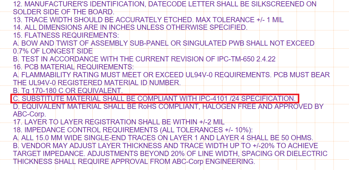
Implementing Option #2 is simple in your fabrication notes. The image below shows an example fabrication note that states clearly which slash sheet your material set must conform to (note 16.C, outlined in red). Note that this can be implmented even if impedance control is not needed.
Within Option #3, your fabrication house may need to adjust these specifications a bit. You will need to specify allowable tolerances on layer thickness and trace width in your fabrication notes. The example below shows how this can be specified as an allowable tolerance for the fabrication house. The red box defines the nominal impedance target implemented in the design as it is initially supplied to the fabrication house. The blue box specifies the allowed tolerances on the trace width and layer thickness
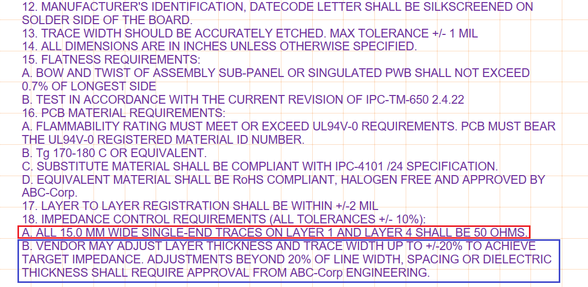
By doing this, you're accounting for the fact that the materials a fabrication house uses may have different dielectric constant than what you used in your design. Because they won't always be able to hit the required dielectric constant, they will have to adjust the trace to compensate for any major difference that brings the impedance outside the specification defined in Note 18.A.
When you're ready to compile documentation for your PCB design and send your manufacturing file package into production, use the autoamted drawing tools in the Draftsman package included in Altium Designer®. Once you're ready to release your fabrication data to your manufacturer, you can easily share and collaborate on your designs through the Altium 365™ platform. Everything you need to design and produce advanced electronics can be found in one software package.
We have only scratched the surface of what is possible to do with Altium Designer on Altium 365. Start your free trial of Altium Designer + Altium 365 today.

About Author
Related Resources


Related Technical Documentation


Take advantage of the world's
most trusted PCB design system.
One interface. One data
model. Endless possibilities.
Effortlessly collaborate with
mechanical designers.
The world's most trusted
PCB design platform
Best in class interactive
routing
View License Options
Thank you, you are now subscribed to updates.