Design Planning with Differential Pair Routing Software and Directive Symbols
Table of Contents
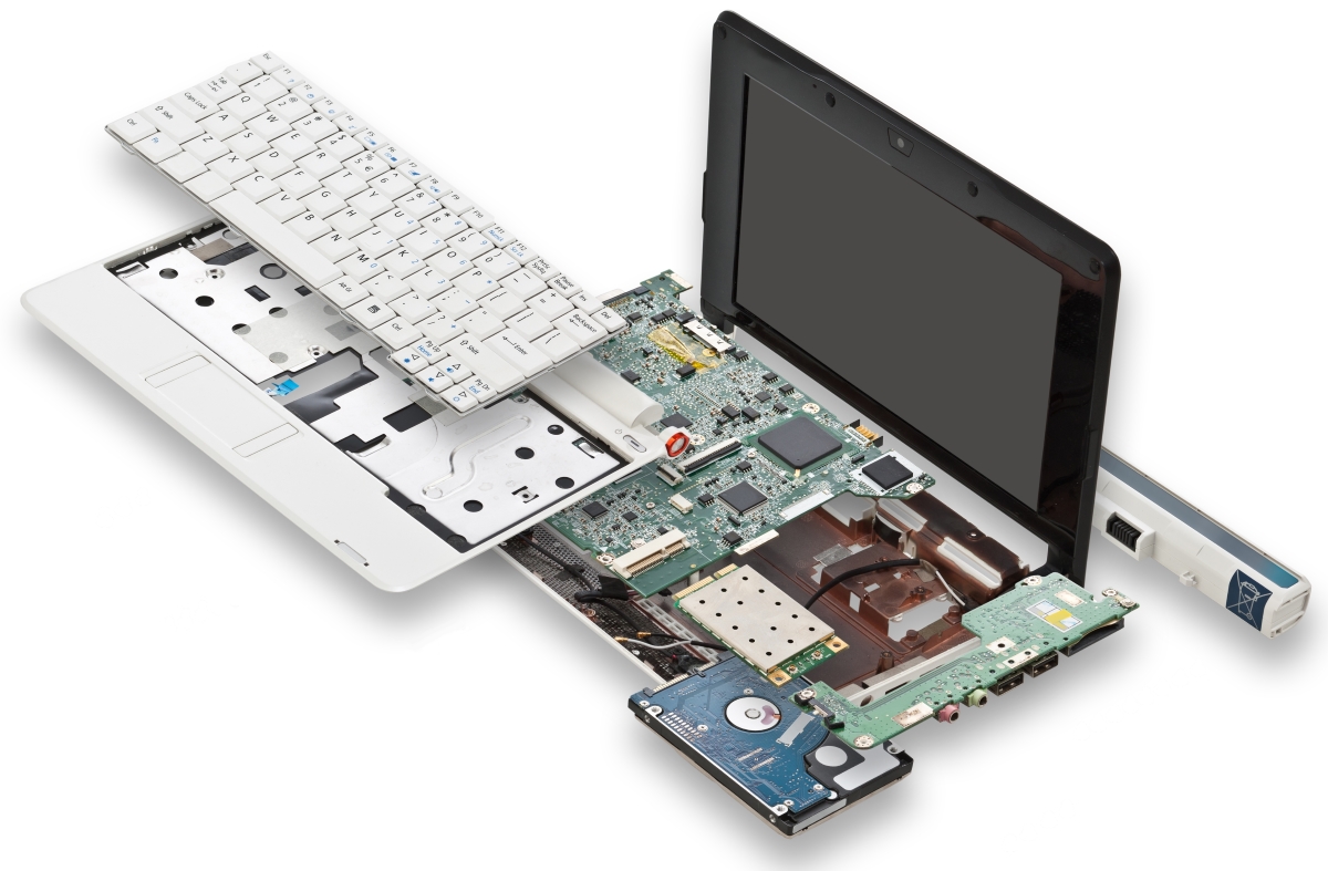
If the components on your PCB are like the organs in your body, then your trace routing between components are like blood vessels. What looks like a complex tangle of copper connections is actually a meticulously designed system that uses well-understood design rules. Your PCB design software can help you maximize your productivity while routing and prevent errors using directive designations.
Great PCB design software doesn’t just let you set design rules and routing directives, it gives you flexibility in how these rules appear in your schematic and layout, customizing routing constraints and directives for your specific application. When you work in a unified design environment, directives defined in the schematic translate easily into the board layout. If your PCB software has these features built-in your routing experience will be quick and easy.
Piecemeal Software Installations Leave Important Functions Out
Some PCB design software packages like to masquerade as complete packages. But in reality, features are separated into different programs or need to be bought as add-ons. This lack of integration doesn’t just sap your productivity, it also costs you money every time you need to buy an add-on feature. You’ll want to ensure that your PCB editor retains the options you need for your circuit layouts.
Your PCB software should let you set layout rules by adding relevant parameters as part of an object's properties. Piecemeal software won’t let you add this information in either schematic or layout, and you should consider yourself lucky if directives transfer properly between layout and schematic. PCB files and options should be there to ensure that your work gets to transfer seamlessly.
Differential pair routing designations and rules exceptions are specified using dedicated design directives. If your PCB design software is incapable of designating and automatically routing differential pairs, you run the risk of routing your traces improperly. Without any sort of design rules or directives checks in place, you could end up routing incorrectly and you wouldn’t even know you have made an error.
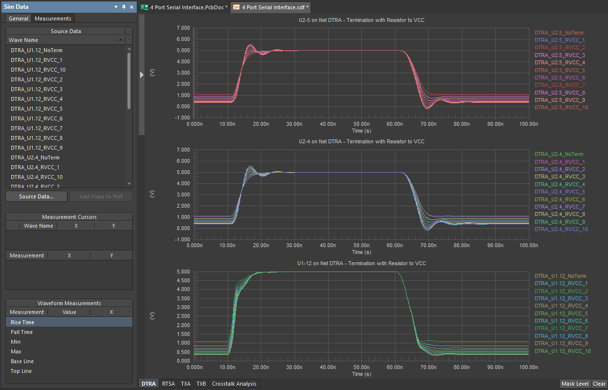
ActiveRoute tool in Altium Designer
Realizing Where the Pain Comes From
When you purchase a PCB design software package, it should actually be an integrated package. No one wants to get halfway through their design just to find out that they don’t have all the tools they need to finish the job properly. Certain piecemeal design packages do not even include differential pair routing features. This is a simple requirement for designing any board, especially if you intend to prevent crosstalk and suppress EMI.
Once you purchase the differential pair routing feature, suddenly the software doesn’t include things like propagation delay rules and compensation features. This prevents you from being able to design anything but the simplest PCBs that you could have already designed using free PCB design software. When working with components like directional couplers, or working through problems like avoiding harmful interference, you’ll want the best software.
If your layout and schematic software are separated, you need to be assured that any design directives are synchronized between the two programs. There is always a possibility for directive errors to occur when moving between your schematic and layout software. This is almost guaranteed to occur when you work in a large organization and transfer your designs across different machines on the company network.
Differential Pairs and Directive Symbols are Reliant on Other Tools
It is unlikely that you are working on a circuit board design with only using one tool. When working on differential pair routing or directive symbol placement, you’ll likely also be relying heavily on constraints editors, design rule checks, and strong library management software. When these other necessary features and tools are part of extra feature packages, much of the consistency and reliability in design predictions becomes left to the whims of financing.
Despite the obvious advantages of using unified PCB design software, some companies still put a major price tag on PCB design packages that don’t even include all the features you need to design high-quality PCBs. When you work in a unified design environment, directives specified in the schematic are easily passed to the layout, and vice versa. Directive symbol placement and differential pair configuration can be performed at either level, giving you the freedom and flexibility to use the software in the way that works best for you.
Your device is, ultimately, the end goal that you want to guarantee works when it leaves your hands. All of the equipment you need to get there, whether it is management of PCB layout or thinking about connected circuits and systems design through your PCB editor, is invaluable in making sure that you’re capable of working through the needs that your design has.
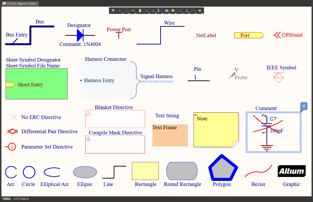
ERC suppression symbols in Altium Designer
Configuring Routing Directives Is Easy in a Unified Design Environment
Altium Designer has found the perfect balance between a powerful routing interface and providing intuitive access to all the routing options you need. Configuration options for differential pair directives are easy to access and apply to each net in your PCB. Once a differential pair directive is placed in your schematic, this directive is easily synchronized with your layout within a single design environment.
Your particular application may call for unconnected pins in your ICs. The No ERC Directive feature in Altium Designer allows you to view and suppress any ERC violations in your design. You can select individual unconnected pins on your ICs and place No ERC Directives on each pin directly in your schematic. The guided process in Altium Designer automatically configures each directive so that specific errors and warnings are suppressed.
A great PCB design software package like Altium Designer can be a major time saver. The ActiveRoute tool in Altium Designer allows you to define your signal nets, select differential pairs, and lay traces automatically. You can customize trace routing constraints and dimensions that are critical for your unique PCB design.
Altium also helps you get support from an active community of PCB design professionals. You’ll have access to the AltiumLive forum, user groups, video library, and webinars provided by industry experts. Altium also maintains a thorough knowledge base and easy-to-read documentation with examples. Altium knows that a strong support network will help you succeed as a PCB designer.
Now you can download a free trial of the PCB layout software that you want to use for your designs. To find out more about Altium Designer and how its routing features can help you design your next product talk to an expert at Altium.


