High-Speed Design: Definitive Guide for Utilizing Altium Designer for Your Board Needs
Table of Contents
There was a time in printed circuit board layout when working with high-speed designs was a living nightmare. Those older CAD tools just didn’t have the horse-power or the functionality to help much when it came to working with the extra design requirements. Differential pairs had to be routed together manually, and measured trace lengths had to be calculated by hand. And if that wasn’t hard enough, trying to determine the total length of a signal path so as to compare it to another was impossible. There were times where I would actually take a ruler and place it on my screen to compare two different lengths of trace.
With high-speed digital design, it couldn’t be more important for your design process that you maintain circuit performance, your power supply, and signal quality. With noise margins being smaller on high-speed designs, the PCB material you might need to maintain a ground plane, capacitors, capacitive loading and clock skew will be paramount to keep track of within your CAD tools.
Thankfully today’s PCB design CAD systems are much better equipped to handle the rigors of high-speed design requirements. This takes the pressure off of you allowing your attention to remain focused on the design and not interrupted by a constant need to consult a hand-held calculator. Altium Designer® is a great example of a PCB design CAD system that provides the with the tools and functionality that they need in order to get the job done. Here is some of what you can look forward to using in Altium on your next high-speed design.
Routing Differential Pairs
Routing differential pairs is an essential part of designing printed circuit boards whether the board is considered to be high-speed or not. Although PCB design CAD systems usually have some sort of help here for diff pair routing, the bad ones can make you want to pull your hair out. Fortunately, Altium has an excellent diff pair routing system which starts in the schematic.
To add diff pair routing information at the schematic level in Altium, use the “Place” pulldown menu and select the “Directives > Differential Pair” command. This will float a diff pair symbol, or directive, on your cursor which you can then place on the net that you want to designate as a diff pair net. By double clicking on the diff pair symbol, you can set up the PCB layout routing rules for the diff pair as in the picture below.
Adding differential pair information to the schematic in Altium
Altium also gives you the ability to add multiple directives in the schematic by using the blanket command. This allows you to select an area where the diff pair directives can be replicated on multiple nets.
You also can add your diff pair rules directly to the PCB rules and constraints. In Altium’s PCB layout editor you can use the “Design” pulldown menu to access the rules or engage the rules creation wizard. Below is an example of some differential pair routing rules from the PCB Rules and Constraints menu.
Setting up the PCB routing rules and constraints for a differential pair
Altium’s layout editor also allows you to directly manage your diff pairs in the differential pairs editor available in the “PCB” panel. This editor will allow you to add, delete, or edit diff pair rules, as well as get statistics on the current diff pair routing. This editor also gives you the ability to create diff pair rules using the differential pair rule wizard button at the bottom of the diff pairs editor menu. The diff pairs rule wizard will guide you through several steps to create a rule including setting up the routing parameters as shown in the picture below.
Altium’s Differential Pair Rule Wizard
Now that your differential pair rules are set up, you are ready to route. By using the “Routing” pulldown menu in Altium you can engage the “Interactive Differential Pair Routing” command. Select one of the nets of the diff pair that you want to route, and begin guiding it along the path that you want to take. Altium will form the traces of both nets maintaining the distance between them as specified in your rules.
Routing a differential pair in Altium
Tuning Trace Routing to Match Specific Lengths
Often in high-speed designs you will need to route traces to a specific length. Usually these lengths are set up in the design rules, and Altium will report this information back to you. To achieve a specified length, or to match the length of the trace to another, you may need to add additional segments to your trace routing. This process is called trace tuning, and once again Altium has the functionality that you need to do this easily.
To tune a trace, go to the “Route” pulldown menu and select “Interactive Length Tuning”. Now click on the trace that you want to tune, and you will see a tuning progress bar displayed. This bar will give you feedback on the tuning that you are doing, but before you continue you should set up some tuning parameters first. To do this press the “Tab” key to pause the routing, and you will be presented with the dialog box that you see below in the properties panel.
Setting up the parameters of interactive trace tuning in Altium
In this dialog, you will see net information on the trace that you are tuning. You have the option here to get your trace length value from either the net, the design rules, or you can manually enter it yourself. For our purposes, we will manually enter our target trace length value. Next, we can set the pattern of the trace tuning which includes setting the style, amplitude, radius, and other values. For our demonstration, we are setting our tuning up to have rounded corners with the values that you see in the picture above.
Once the tuning parameters are finalized, you can go back to the design window and click on the “Pause” symbol to continue routing. By hovering the cursor over one end of the trace and then moving it, you will add extra segments into the trace causing its length to increase and thereby “tuning” it. In the picture below you can see how by moving the cursor up the trace segment, rounded tuning segments were added in. You can also see the beginning of the green status indicator being displayed in the progress bar to show how much tuning has been accomplished, and how much more is needed.
Interactive trace tuning, move the cursor up to add length
Routing Signal Paths in High-Speed Design
Even when PCB design CAD systems first started reporting net trace lengths, there was still wasn’t a way for designers to work with the entire signal path length. A signal path example involves multiple nets starting at a driver, going through other components, and then terminating at a load. Designers used to have to keep track of the individual net lengths and perform manual calculations in order to get their signal paths at the correct lengths while at the same time visually managing routing topologies to ensure that they were correct. It was an enormous challenge to say the least.
Altium Designer has provided a solution for this need with its “xSignals®” functionality. With you can track and report the individual nets and trace segments within a signal path to control the timing of the signal by matching routed lengths. will also handle different high-speed routing topologies, and will work with the design rules for interactive length tuning and differential pair length tuning. also contains a technology-aware wizard which will automatically create the , xSignal classes, matched length groups, diff pair matched length rules, and routing topologies for technologies such as DDR3 and DDR4 circuitry.
Creating an rule by selecting component pads in Altium
There are many different ways to work with in a design. In the picture above we have selected several component pads connecting different nets that are all part of one signal path. With the right mouse button popup menu, we then create our signal path by going to “ > Create xSignal from selected pins.” This will highlight our signal path and open the menu as you can see below.
The highlighted signal path and the menu
With you have a lot of control over your signal paths. In the picture below you can see that we have selected some of the trace segments in our signal path. You can see where the first net comes from the driver pin to the left side of the resistor, and then the second net comes from the right side of the resistor and continues on. The menu reports net names, segment lengths, total signal path length, and much more.
Selected signal path trace segments in Altium ’s
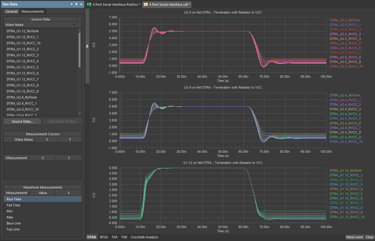
There’s a lot to high-speed design from eliminating crosstalk in your design to understanding what the best termination methods are to use. Checking characteristic impedance, data rates, and return path in high-speed applications, or finding propagation delay and radiated emissions will be a breeze when your circuits are developed in strong software.
Fortunately, Altium can help you with all of this. Starting with signal integrity analysis in the schematic, through board layer stack creation and layer stackup management, to high-speed routing features, and all the way through the final manufacturing output files, Altium is the PCB design software that you need to get the job done right.
Would you like to find out more about how the power of Altium can help you in your next high-speed design? Talk to an expert at Altium.


