Use Interactive Routing to Mitigate EMI Issues from High-Speed PCB Traces
Table of Contents

Having a robot clean the house and perform laundry chores continues to elude modern technology given intricate steps to complete each chore. Given the repetitive nature of the chores, you’d think robotic automation would be the perfect application to turn over to a robot. It turns out that cleaning the house and doing the laundry is much more complicated and too advanced for robot understanding.
Only simplistic chores, like vacuuming the floor, are within reach of robot intelligence. Using autoroute with PCB layout tools continues to escape automating more than simplistic and careless net placement. Given inadequate programming tools to deal with complexities of PCBs, the autoroute feature in most PCB layout packages fails when reason is needed to place nets and vias elegantly.
The simplistic ways of literal algorithms return odd choices for vias, nets, and their relative places within the layout. This leaves PCB designers holding the bag, left to meticulously discover and manually resolve the wonky results of autoroute algorithms. Ground loop, interference, impedance, or even just the basics of finding electromagnetic compatibility can be left feeling unresolved.
Literal Autoroute is Simplistic and Takes the Wrong Way
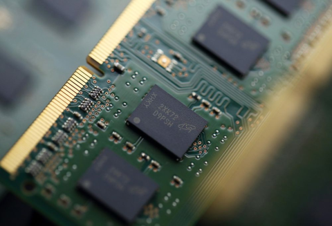
After placing components and activating autoroute, the result is reckless. The layout is full of unnecessary vias and meandering nets. The time saved by using autoroute is now wasted with a layout that is unusable without lengthy manual intervention. The resultant layout, if used, would cause expensive manufacturing. A printed circuit assembly built with too many vias and loopy nets would most assuredly exhibit EMI issues when engineers compliance test.
When I’m looking at any circuit, or even high frequency designs, I know that noise and interference are going to be strong on my watch radar. But ground and power issues can play just as important role when it comes to routing: have the traces I’ve laid out been placed well enough to allow for my board’s demands?
A PCB built and assembled with immature autoroute placements is low quality. Having a powerful PCB layout tool that produces low quality PCBs leaves the designer scrambling for time to meticulously check and resolve inadequate solutions. The solutions were instantiated with autoroute tool and given complex designs, a great deal of time and expertise is required to resolve the issues. The rules and constraints set up before autorouting failed to incorporate, literally translating and applying in odd ways.
Wrangling Vias and Routing Oddities Disrupts the Flow
Helping autoroute by anticipating rules before net placement requires blind faith and an impossible ability to predict intricate details of a PCB layout before they occur. Having to populate the rule and constraint editor outside of the layout environment makes it prone to omissions. Leaving a layout to reopen the rule editor can cause other details of the design to be overlooked. Keeping track of where the design stops and starts is distracting.
Reviewing autoroute result after defining rules and inspecting results produces disappointment. The number of vias and meandering nets is disturbing. Manual work will be necessary to resolve. After resolving the most glaring errors, meticulous inspection follows to discover any other oversights. Steps such as removing ground nets and plane layers to make copper pours are required before adding grounds back into the layout. Each layer must be inspected to identify and clean up oddities as a result of autoroute.
All of this wasted time from a tool intended to save time. It’s the age-old dilemma: when stuck in traffic on the highway, do you get off the highway and take a much longer route or do you stay on and stick out the traffic? Except the loop area we’re talking about is a bit different than a traffic loop, the ground we’re on is not a road, and the noise we’re hearing is not traffic horns.
Use a wizard’s magic to unleash interactive flow
Shape-Based Intelligent Routing for Easy Features
It would be infinitely better if the tool allowed interactive process steps while running autoroute alongside detail definition. That way, specific sections and details could be refined before running autoroute on that section of the layout. The environment would allow implementation of rules and definitions throughout layout at the moment they are top of mind. This would ensure details are captured before autorouting.
The simplest request is to have a tool which saves a designer time. Most likely I’ll be spot-checking anything I receive from an autorouter, but I’d love it if my routing tool could make my time spent spot-checking particularly efficient. Highlighting problem areas or running through an engine that was updating your board in real-time based on frequency, radiated EMI, power and noise demands.
In addition, the tool would use shape-based intelligence so layers are understood by the router when initially defined. With shape-based intelligence the router would recognize and implement need for elegant via placement, reducing unnecessary vias as a result of autoroute. In addition, given that routing is critical for quiet boards, free of electromagnetic interference, the tool would provide impedance calculators at the time they are needed taking the guesswork out of when necessary rules require definition.
Auto-Interactive Routing Resolves Routing Issues
It turns out that Altium Designer 18 incorporates an interactive routing design environment that defines intricate net rules and layer stacks before unleashing autoroute. Setting up and defining nodes of interest can begin in AD 18’s schematic capture tool, setting up the PCB layout for successful autoroute.
Altium Designer 18 offers a wizard to ease setup of critical signal traces
The PCB layout environment provides access to an xSignal Multi-Chip Wizard (see above-two illustrations) from the “Design” pulldown. The beauty of this tool is its easy accessibility from the layout. With easy access you can set specific rules within the wizard and check results before moving onto other areas of the layout.
In addition, the Layer Stack Manager defines the layers for interaction with autoroute. Defining the layers and having them recognized by autoroute sets up the design for electromagnetic compliance. In addition, the Layer Stack Manager incorporates an Impedance Formula Editor within the tool so high-speed signals can be analyzed to set their critical impedances. This results in the signal integrity for your layout by avoiding reflections, ringing, and cross-talk.
Moving on to signal integrity tools, also easily accessed from the pulldown, layouts can be checked for reflections, ringing, and cross-talk. With access to graphic signals, any tweaks to improve designed signals may be made in the layout before releasing gerbers for fabrication. We all want to manage noise, signal, and frequency issues in our designs. It’s time to use software that can plan both power, shielding and conductors and noise and frequency matching.
Altium Designer 18 is a powerful and easy-to-use Schematic Capture and PCB layout tool that incorporates an interactive router for sensitive signal definition. Its xSignal Multi-Chip Wizard and Layer Stack Manager provide intuitive tools to get your nets placed well.Its unified environment makes it easy to use, getting you to the results you need for signal integrity within your designs before the PCBs go to manufacture.
If you are looking for an EDA tool that includes easily used tools for designing your PCB layout with intelligent net routing, talk to an expert at Altium.
Start the journey to switch over to Altium Designer today.
“My productivity has never been higher!”
- Consultant at Service Company
Related Resources


Related Technical Documentation


Take advantage of the world's
most trusted PCB design system.
One interface. One data
model. Endless possibilities.
Effortlessly collaborate with
mechanical designers.
The world's most trusted
PCB design platform
Best in class interactive
routing
View License Options
Thank you, you are now subscribed to updates.