PCB EMI/EMC Guidelines: Meeting EMI/EMC Standards in Your Designs

What if you set two cell phones next to each other and suddenly neither of them worked properly? Thankfully, this doesn’t happen because designers and manufacturers made serious efforts to ensure these devices comply with EMC standards on conducted and radiated EMI. Any device should comply with EMC standards before it makes it to the marketplace.
While this sounds complicated, you have a number of simple design strategies to help your next device pass EMC tests. Making yourself aware of the various EMC standards organizations and their specifications is a good place to start.
EMC/EMI Standards for PCB Design
EMC standards fall into two broad categories: regulatory standards and industry standards. The regulatory standards for your design depend on where you want to market and sell your product (not necessarily where it is designed or manufactured). Some of the earliest EMC standards were established by the U.S. Federal Communications Commission in 1979. The European Community later defined their own EMC standards, which formed the basis for future European Union standards, now known as the EMC Directive - officially named Electromagnetic Compatibility (EMC) Directive 2014/30/EU of the European Parliament (you can view the European standard here).
Conformance to industry standards is not just a legal matter, it is also an industry-specific matter to ensure uniformity and interoperability among electronic equipment deployed in specific environments and application areas. Effectively, industry EMC standards play the same role as other industry standards on manufacturing, assembly, performance, etc. The major industry standards organizations and regulatory bodies defining EMC requirements include:
- U.S. Federal Communications Commission (FCC)
- U.S. Federal Aviation Administration (FAA)
- Underwriter Laboratories (UL)
- American Radio Technical Commission for Aeronautics (RTCA)
- International Electrotechnical Commission (IEC), through Comité International Spécial des Perturbations Radioélectriques (CISPR)
- International Organization for Standardization (ISO)
- Society of Automotive Engineers (SAE)
- Institute of Electrical and Electronics Engineers (IEEE)
- The U.S. military through its MIL-STD set of standards
While IEC and CISPR standards are more popular in Europe, IEEE standards are more popular in the U.S. In particular, the IEEE standards forms the basis for antenna calibration tests. The MIL-STD EMC requirements are among the most stringent standards worldwide and were some of the original standards being adapted to the commercial sector for electronic devices.
Broad Requirements for Complying with EMC Standards
Companies caught releasing non-compliant devices or products might receive a warning, or be fined substantial sums of money. Failure to meet EMC requirements also poses a safety concern and damages a company’s reputation. Designing with an eye towards EMC can help ensure you won’t receive civil penalties once your device comes off the fabrication line. Designers take steps to comply with EMC standards by considering EMI from two perspectives:
-
Designing for EMI immunity: Design a device to withstand unwanted EMI from nearby devices. This typically starts with the right stackup and routing strategy.
-
Suppressing radiated EMI: Design a device to minimize the radiation it emits. The layer stack, grounding strategy, component placement, and possibly shielding all play a role here.
-
Suppressing conducted EMI: Conducted EMI takes several forms, such as coupled common-mode or differential mode noise, switching noise from SMPS regulators, or harmonics received from the grid.
-
Fast transients or power fluctuations: These types of noise appear as series of injected pulses, brief voltage dropouts, periodic dropouts, or power spikes. The design should prevent these from appearing as noise on an output or load. These requirements are applicable on designs with short cables or AC inputs, respectively.
-
Suppressing surges and ESD: We generally focus on noise when discussing EMI/EMC, but withstanding surges and ESD are also important aspects of designing to comply with EMC standards.

Radiated EMC measurement with a near field probe
Some Strategies for Increasing Your Chances of Passing EMC Standards Tests
There are some basic design practices every designer should use to ensure their boards pass even basic EMC checks.
Stackup, Power, and Grounding
An EMC compliance strategy starts with your layer stack. Designing your board with a low inductance ground system has the greatest effect of minimizing EMI susceptibility. With multilayer boards, you should place a ground plane directly below signal layers in order to minimize loop inductance.
Interference in low-level signals leads to lower signal-to-noise ratios. So, it is a good idea to route these signals on an interior layer. If you have enough layers in your stack, place these traces between two ground planes, and then place your power plane below the bottom-most ground plane. Placing the power plane close to the ground plane provides strong capacitive coupling. Any noise or conducted EMI in the power plane will easily bleed into the nearby ground plane rather than interfering with signals.
Be careful when routing signals from an interior layer up to a surface layer as you will need to maintain tight coupling. You can maintain coupling to a reference plane by placing a nearby parallel via between the ground plane and the surface layer. Other EMC problems like clock routing and placement can be problematic and create excessive noise, particularly when changing reference planes in a multilayer PCB. If you can help it, try not to use protocols that require an external reference oscillator, and instead use protocols that have an embedded clock. Some protocols like DDR use a source-synchronous differential pair clock, which will have lower radiated EMI than a single-ended clock connection (see below regarding differential pairs).
Incorporating Shielding
Judicious use of shielding is another strategy to provide your board immunity to radiated EMI. This also suppresses EMI radiated away from your board. If you are working with a wireless device, you can just place the antenna outside the shielding so it can still send and receive signals.
The simplest solution is to just use grounded shielding which will form a Faraday cage around sensitive components and traces. Not all designs and components will accommodate this solution. So, you might require a more elaborate shielding method. If you use a uniform ground plane in the interior of your board (you should do this anyways), a grounded via fence around the edge of your board and via stitching on copper pour regions will provide similar protection.
Shielding can for suppressing radiated EMI
Shielding cans are probably the most common form of shielding that everyone thinks of, it's not the only possible type of shielding that can be used to combat EMI. Other unique shielding materials that can provide broadband EMI suppression include:
- Conductive foam or elastomer gasket materials that absorb RF emissions
- Wire mesh materials that can be mounted to the enclosure
- Metallic tapes that can be used for mating surfaces or some places on the board
- Conformal coatings with absorption in a problematic frequency band
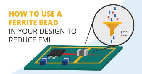
- Ferrites that can be attached directly to the enclosure or cable assemblies
These other types of shielding can be implemented on the board or in the enclosure when other solutions used on the PCB fail. Personally, I would only recommend shielding cans and some of these other materials be used only after implementing the gamut of board-level solutions.
Mixed-signal Layout and Routing
Some devices may need to manipulate digital data and support analog signaling, making them inherently mixed-signal devices. It is a good idea to try and separate digital, low-frequency analog, and RF analog sections of the board into different regions of the PCB layout. It's always good to ensure these sections have their own dedicated areas in the ground layer, but the ground layer should be kept continuous. This means the challenge here is to track the return path around the board. The goal is two-fold: prevent interference between different board sections while also ensuring signals do not have huge loop inductances by routing them over ground on the adjacent layer. To learn more about mixed-signal grounding strategies, read this article.
Bypass/Decoupling Capacitors on the Power Bus
Last but not least, understand that power bus noise creates EMI, which can be radiated from the board edge. This requires proper stackup design, bypass/decoupling capacitors placement, and reference/power plane pair placement. Reduction of noise on the power bus in advanced digital systems with many I/Os is as much a power integrity problem as it is an EMI/EMC problem, so focus on understanding the fundamentals of power integrity to deal with these problems.
Designing towards EMI/EMC standards for PCB design requires the right layout tools to implement board-level solutions. Altium Designer® provides everything you need to create a compliant layout or perform rework as needed. Altium Designer is the industry’s leading CAD platform that also provides integration with cutting-edge applications for SI, PI, and EMI/EMC simulations. When you’ve finished your design, and you want to release files to your manufacturer, the Altium 365™ platform makes it easy to collaborate and share your projects.
We have only scratched the surface of what’s possible with Altium Designer on Altium 365. Start your free trial of Altium Designer + Altium 365 today.

About Author
Related Resources


Related Technical Documentation


Table of Contents
Take advantage of the world's
most trusted PCB design system.
One interface. One data
model. Endless possibilities.
Effortlessly collaborate with
mechanical designers.
The world's most trusted
PCB design platform
Best in class interactive
routing
View License Options
Thank you, you are now subscribed to updates.