Beginner’s PCB Design for Manufacturing Guidelines

Table of Contents
Design professionals talk a lot about design for manufacturing guidelines, but what exactly are these and how are they implemented in your PCB design software? In PCB development, design for manufacturing has a very simple meaning: you should only implement design choices if you can ensure they are manufacturable with maximum yield. This deceptively simple explanation leaves out a lot, and it’s natural to assume your fabricator can manufacture anything you put into a PCB layout in your design software.
The truth is that different fabrication houses have different capabilities, material options, and standard no-touch service options. There are some very common mistakes or oversights that will cause a board to be un-manufacturable and could create the need for extensive redesigns. In this article, I’ll run over some of the most common mistakes that might be made by new and experience designers. I’ve made these mistakes myself, but I can tell you can always recover from these mistakes and ensure your board will be manufacturable.
Some Basic PCB Design for Manufacturing Tips
The points I’ll outline below relate almost entirely to two important areas:
- Material considerations, specifically core/laminate materials and copper weight
- Fabrication limits, specifically features sizes and spacing in a PCB layout
With that in mind, let’s jump right in and start looking at some of the fundamental PCB design for manufacturing guidelines you’ll need to ensure design success.
Get a Layer Stackup First
You would be surprised how easy it is to just jump into your new design and start placing components around the board. For simpler boards that don’t require controlled impedance, specific bus capacitance, or dense digital routing, it’s possible to just start placement on an even layer-count board with standard layer thickness. Depending on the design, the manufactured PCB may not create the functionality you expected.
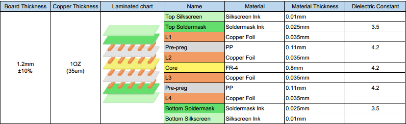
With most designs, even on microcontroller boards for hobby usage, you’ll at least need to know the layer arrangement and material properties. Email your fabrication house and get a standard layer stack before you start designing traces for digital buses or any controlled impedance traces. If you don’t, the fabrication house might produce your board using a layer stack that does not produce the functions you expected. The other risk is that you create a layer stack that they can’t manufacture, usually because there are no material stocks that match your stackup specifications.
Match Copper Weight to Current Density and Laminates
When you’re selecting materials or getting a stackup approved, don’t be surprised if your fabricator pushes back on your copper weight. You need to use copper weights that are available on your fabricator’s material set, you can’t just specify any copper weight you want. If you took time to estimate the copper weight and trace width you need for a particular current density (such as on power rails), then you should make sure to specify the required weight when determining the stackup with your fabricator.
Enforce Copper-to-Copper Clearances
When you start a new PCB layout, your ECAD software will apply a set of default clearance rules that are conservative values for just about any PCB. These values are usually overly conservative, so it’s common to just ignore them without programming in the correct clearance values before starting the layout. Worse yet, you might enter in values that are too small, which will allow you to place elements too close together such that the board cannot be fabricated.

The solution: get your fabricator’s limits before you start placement and program these values as design rules into your PCB project. If you want to make sure you hit the most common clearance violations, focus on these clearances:
- Trace-to-trace
- Trace/pad to polygon
- Trace-to-pad
- Pad-to-pad
The last two points will apply to SMD pads and landing pads for through-holes (vias or component leads). Note that these values will be larger for heavier copper due to the need for etch compensation.
Overlapping Drill Hits
If you followed the previous clearance guidelines and set your minimum pad-to-pad spacing values, then you might have already addressed this design for manufacturing guideline. If drill hits are spaced too close together, it is possible they could overlap each other due to wander in a CNC drill. Every drill hit will be slightly off-center from its ideal hit location, and this needs to be accounted for when placing vias and through-hole leads.
Note that, even if you obey pad-to-pad clearances for vias and through-hole leads, this might not guarantee you’ve satisfied a drill hit clearance. Suppose you place a 10 mil via with a 12 mil pad; if your pad-to-pad spacing limit is only 5 mils, but your drill-to-drill spacing is 10 mils, you’ll violate the drill hit limit by 3 mils if you only follow the pad-to-pad limit.
A similar problem can occur between drill hits that pass through a plane, such as the thermal relief and the GND plane clearance shown below. The two green regions show the clearance between the via wall and a plane for these nets; the leftover sliver here is very small and will not be manufacturable. The specific example shown below is one instance where such a fabrication failure will not cause the device to be non-functional, but this may not be the case in general. If such a defect were on the surface layer between two through-holes, this would create a risk of bridging during soldering as the narrow copper feature would likely be etched away during fabrication.

The natural solution here is to just use a larger pad, which is exactly what you would do to satisfy basic IPC class requirements; use a minimum pad size of (drill diameter) + 8 mils to ensure you’ll almost always satisfy the drill-to-drill clearance limit.
Small Feature Sizes
When you start packing components and traces into a board, there is a temptation to start making traces, drill hits, and pads unnecessarily small. Clearance rules will already limit how close you can pack everything, but an equally important design requirement is minimum feature sizes. The two most common points you’ll need to address are minimum hole sizes and trace widths. This point is as simple as looking up fabricator feature sizes and programming them into your design rules. Typical fabrication limits that apply to most boards are 4 mil trace width and 6 mil drill hole width. For many simpler boards that do not need controlled impedance, it's best to use 8-10 mil trace width and 10 mil drill diameter.
Solder Mask Slivers
This is an often-overlooked aspect of assembly that is intended to ensure solder mask openings can reliably function as a dam against molten solder flowing between two nearby components. Even though pads may be spaced out appropriately, an excessively large solder mask opening on an NSMD pad will can leave behind a very thin channel of solder mask between the pads.

A typical minimum solder mask sliver requirement here is 5 mils. When the solder mask sliver is below the fabricator’s limit, it might snap off after it is cured, and it creates a channel where two pads could be bridged with solder. The solution here is to apply additional spacing, or to reduce the solder mask opening on the affected pad so that a sufficiently large sliver remains.
Overlapping Silkscreen
After placement and routing is finished, the silkscreen should be inspected to ensure there are no overlapping reference designators. If there are, you can move these around in the PCB layout until everything is clear. While not technically a requirement for successful fabrication or assembly, a diligent manufacturer will still flag it as a problem during a design review.
A more important problem is overlapping silkscreen with pads/holes where solder will be applied. Make sure to check for this, either with a 3D model viewer or by looking at the Gerbers directly.
The above list of guidelines should address the most common DFM problems that can affect almost any designs. When you implement the above guidelines in your projects, it will become part of the normal design process. Once these points are programmed into your design rules, you can check them at any time as part of a design review before you put your board into production.
When you need to access an easy-to-use PCB layout tool that includes everything needed to build high-quality manufacturable circuit boards, look no further than CircuitMaker. In addition to easy-to-use PCB design software, all CircuitMaker users have access to a personal workspace on the Altium 365 platform. You can upload and store your design data in the cloud, and you can easily view your projects via your web browser in a secure platform.
Start using CircuitMaker today and stay tuned for the new CircuitMaker Pro from Altium.
Check out Altium Designer in action...
Powerful PCB Design

About Author
Related Resources


Related Technical Documentation


Take advantage of the world's
most trusted PCB design system.
One interface. One data
model. Endless possibilities.
Effortlessly collaborate with
mechanical designers.
The world's most trusted
PCB design platform
Best in class interactive
routing
View License Options
Thank you, you are now subscribed to updates.