PCB Design Guidelines for Analog Circuits

Table of Contents
Even though building analog systems might seem like going back in time to the days of vacuum tubes, analog components and circuits are not going away any time soon, nor are the PCBs needed to support them. Purely analog circuit boards and mixed signal PCBs will remain important in many products and will continue to operate at a range of frequencies. Getting started with PCB design rules for analog circuits can be difficult in terms of where to begin and what to think about, but we hope that these guidelines will help you understand the steps you can take to ensure success.
Sometimes, it's best to think about analog PCBs and mixed-signal PCBs in terms of a common design goal. Analog circuits and PCBs need special care as the goal is generally to route signals and input them into components/circuits while ensuring low-noise operation. Then, the frequency range at which the board operates will determine some of the measures that need to be taken to ensure the design operates as intended. In this guide, we'll outline some of the standard analog PCB design guidelines you should consider. We'll try to cover from low kHz frequencies up to high mmWave frequencies.
Analog PCB Design Guidelines: Layer Stackup
Once you've designed your circuits, your layer stack is the first step in your design. An analog layer guideline generally follows the same ideas used to build a digital PCB stack-up. Pay attention to these points:
- Power and ground: Plan to use plenty of ground-around traces that carry critical signals in your PCB layout, and plan your power rail routing accordingly. Newer designers might be accustomed to thinking about how they want to route important analog interconnects, but if you do this early you can plan your power and signal routing accordingly.
- Power at high frequencies: If your analog circuit board will need to transmit at high output power and high frequencies, then you need to supply very stable power, possibly at high currents. Instead of rails, plan to use a power plane on an internal layer and place a ground plane on an adjacent layer.
- Material selection: I think every designer would prefer low-loss PTFE-based laminates for every layer in their analog boards, but these costly materials are not always necessary. If you're not operating at dozens of GHz and you're only using short routes, then you will likely be fine with a standard FR4 laminate as long as you are not routing very long interconnects. If you do need a low-loss laminate, contact your fabricator about using a hybrid PCB stack-up.
Today's analog boards often contain a digital section on the same board as the analog section. How should you deal with these in your stack-up? The recommendations for power and ground are generally different in mixed-signal PCBs, and it depends on whether your analog and digital sections need to have any direct routing between them.
Mixed-signal Grounding
If your board will also has a digital section, things get more complex in terms of your component placement. Generally, due to the speed of digital circuits, you should not use physically separated ground planes, you should instead use a single ground plane. Try to plan out your layout so that return paths from the digital and analog blocks are naturally separated. This is difficult at low frequencies, which is why so many design guidelines continue to advocate using separate analog and digital ground planes.
Mixed-signal Power
For mixed-signal power, the power plane is normally split into digital and analog circuit sections, similar to what would be done with a digital power plane operating at different supply voltages. These sections should be in the same layer and referenced to the same ground plane on an adjacent layer. In addition, it's best to put the digital power rail only in the digital section of the board and do the same for the analog circuits power rail.
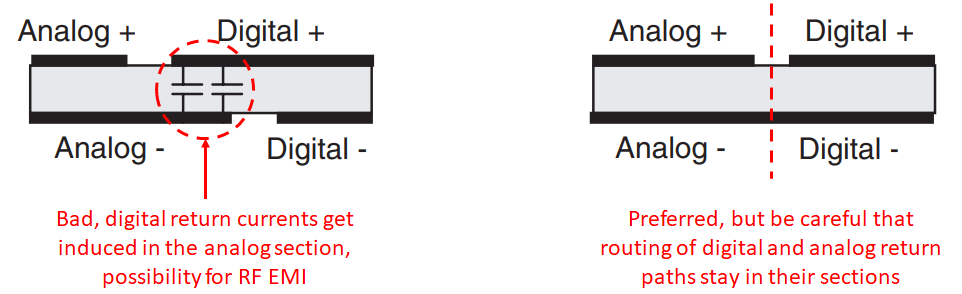
If you must use the arrangement on the left side of the above image, what you should not do is put separated digital and analog power planes in two adjacent layers such that the planes overlap. If these two planes do overlap in adjacent layers, the two planes will have high capacitance between the overlapping areas that creates strong displacement currents. This can then cause cavity emissions at RF frequencies as the potential between these two planes fluctuates during switching.
In addition, you should not create an interface between the digital and analog sections by routing over the gap between the analog and digital sections. To see why to take a look at this article. The interface you need can be provided by an ADC, which might be built into your host controller, or it could be a dedicated IC.
Component Placement in an Analog PCB Layout
Just like the above PWR/GND plane diagrams imply, only put analog components in your analog circuits section, and only put digital components in your digital section. Unfortunately, we can't cover the placement of every possible component, but there are a few important ones we can discuss briefly. Two of the most interesting components that carry some important layout guidelines are ADCs and amplifiers (including op-amps). While I would love to mention PLLs here, these circuits rely on a lot of clock routing and precise timing, which is best left for a separate article.
Dealing with Unused Op-amps
One component that is bound to appear in an analog circuit board is an operational amplifier. In many op-amp ICs, some of the op-amps will be left unused. Any unused leads on the IC should be terminated properly. Unterminated (i.e., floating) leads on op-amps in an IC can produce noise that propagates into the operating ICs, degrading signal integrity.
If you are using a single power supply rail, you should first short the output back to the inverting input. This creates negative feedback and ensures that the output will properly follow the input. Next, connect a voltage divider with equal resistors to the non-inverting input and the ground pin. This will set the input potential to the midpoint of the linear range. If you are using a split rail, you can simply short the output to the inverting input and ground the non-inverting input.

The Trouble with Power Amplifiers
At low frequencies, amplifiers won't be subject to any special constraints that don't apply to any other PCB. For power amplifiers running at high frequencies, the situation is different as there is the potential for instability in the amplifier output, which manifests itself as unintended positive feedback. There are some simulations you can use to track coupling back into the amplifier input, although these require a field solver that can interface directly with your PCB layout. To learn more about this interesting signal integrity problem involving RF power amplifiers, read this article.
Where to Place ADCs
An ADC is where your analog circuit signals will interface with the digital world, so this section needs to be placed carefully as it will have a digital portion. Discrete ADCs are best placed roughly along the boundary between your digital and analog circuit sections. In fact, this is probably the only acceptable way to create an interface in a mixed-signal system that has split ground planes, simply because the ground plane on the silicon die can provide the reference plane for the incoming/outgoing signals. However, if you use a uniform ground plane, you'll have much more flexibility to place an ADC, as well as shielding provided by the ground plane.
Routing Guidelines for Analog PCBs
Routing in an analog PCB is all about ensuring the analog signal sent along an interconnect is not significantly distorted at the receiver side of the interconnect. When working with analog PCBs, you'll typically have a much lower net count than in a digital PCB, so you can experiment with some possible layouts early until you figure out a floor plan that is solvable. Here are some routing guidelines to help you along:
- Trace length: In general, try to keep traces in your analog PCB short and direct, this is quite important as signal frequencies get higher. Pay attention to the critical length of your signals in addition to losses.
- Enforce impedance matching: Even if your trace lengths are very short, it's still a good idea to enforce impedance matching anyways. This might mean you'll need to design some impedance-matching networks on important circuits or components to ensure reflection-less power transfer between circuits.
- Consider coplanar routing: You can take advantage of coplanar PCB routing to ensure high isolation without sacrificing impedance. As I'll show in an upcoming article, you can still enforce impedance control while violating the "3W" clearance rule on the copper pour.
- Minimize use of vias: Each via adds loss to an interconnect's S-parameters, so it's best to minimize these and only make necessary layer transitions if possible. For those vias that do remain, it's possible they can act like antennas that radiate strongly. Read this article to learn more.
Depending on the main frequency you'll work within your board, you might consider routing through an internal layer between plane layers. Higher frequency stripline or coplanar routing on internal layers is preferable when isolation is needed as long as via transitions are minimized. Also make sure your vias are appropriately sized and spaced from planes with antipads for your operating frequency, although this is easier said than done and can't be easily calculated. This particular point should be examined with measurements (S-parameters) as nearby planes and other conductors will modify the via impedance during the signal transition into inner layers.
There's a lot to think about in an analog PCB layout, but the right design tools and rules-driven design software will help you implement the analog PCB design rules for digital circuits you need to keep your analog circuit system noise-free and ensure signal/power integrity. Altium Designer® contains the best PCB layout features for any analog, digital, or mixed-signal PCB in a single design environment, including powerful routing tools to help you stay productive.
We have only scratched the surface of what’s possible with Altium Designer on Altium 365. Start your free trial of Altium Designer + Altium 365 today.

About Author
Related Resources


Related Technical Documentation


Take advantage of the world's
most trusted PCB design system.
One interface. One data
model. Endless possibilities.
Effortlessly collaborate with
mechanical designers.
The world's most trusted
PCB design platform
Best in class interactive
routing
View License Options
Thank you, you are now subscribed to updates.