Pin-Package Delay and Via Delay in High Speed Length Tuning

Table of Contents
Take a look at the inside of some integrated circuit packages, and you’ll find a number of wires bonded to the semiconductor die and the pads at the edge of the component's package. As a signal traverses makes its way along an interconnect and into a destination circuit, signals need to travel across these bond wires and pads before they are interpreted as a logic state. As you look around the edge of an IC, these bond wires can have different lengths, and they incur different levels of delay and contribute to total jitter. Even if a bond wire is not present, the pin size and package will contribute some delay to the signal.
Vias can also induce some delay on any interconnect, which is a function of the via’s length, its inductance, and its capacitance. Signal behavior on vias can be quite complicated to describe analytically, particularly when you start looking at higher frequencies and evanescent coupling along the edge of an interconnect. With some simple pieces of information, you can compensate for pin-package delay and via delay in your PCB interconnects.
Pin-Package Delay in Length Tuning
All signals, whether electrical or optical, travel at a finite speed. This means any section of an interconnect which a signal must traverse will incur some travel time. The bond wires in an integrated circuit, solder balls on a BGA component, pins on a through-hole component, and any other piece of metal that separates a trace and semiconductor die requires some time to traverse, and your designs should account for this delay during length matching.
Pin-package delay is the time required for a signal to traverse the pad and bond wire of a component. IC manufacturers that are worth their brand name will measure this and provide the delay value in the component datasheets; these delays are usually on the order of tens or hundreds of picoseconds. As an example, pin-package delays in some Xilinx FPGAs can vary from 80 to 160 ps.
You’re probably wondering: why do we need to worry about this? The simple answer is that this should be included in the total propagation delay for an interconnect to ensure accurate length tuning. In differential signaling standards, the pin-package delay will theoretically affect both signals to the same extent, so it may be safe to ignore pin-package delay unless operating with rise times <100 ps. With a specialty high-speed standard operating in parallel (such as that implemented in an FPGA), you will need to ensure matching across the bus within your skew margin.

With relatively slower signals (>1 ns rise time) and slower data rates (<500 MHz), you might not need to worry about the pin-package delay in an interconnect, especially if you have a large noise margin at the receiver and are working at a higher voltage (e.g., 3.3 V core voltages). 500 MHz is generally taken as the lower limit on data rate beyond which pin-package delay should be included. Beyond this data rate, the signal repetition rate will be less than 2 ns, and the signal rise time will be even faster. This creates a situation where the pin-package delay is comparable to the data repetition rate and the rise time, and signals could completely desynchronize simply by travelling over bond wires and component pads.
Calculating Via Delay
The signal speed across a via depends on a number of factors, including the pad-antipad distance, the fiber weave effect through the board cross section, and plating imperfections along the length of the via (especially in high aspect ratio vias). Vias that make a layer transition while changing reference planes will also see a sudden impedance and propagation delay change across the length of the via. If we just consider a through-hole via in a 1.57 mm FR4 board with Dk = 4, the one-way via delay is about 10 ps (if we assume uniform dielectric constant across the length of the via), but this number is actually incorrec. In a real via, the delay will be much different, depending on which layers are traversed and on the presence of nearby conductors (i.e., due to parasitic inductance and capacitance with respect to nearby planes).
The challenge in calculating via delay, or the amount of time a signal needs to travel along a via, arises when determining the effective dielectric constant seen by signals traversing the via. You can then calculate the signal speed through a via using the speed of light in vacuum:

Getting an analytical expression for the effective dielectric constant is not trivial. Bert Simonovich presents an excellent discussion of this on his blog (read the article here), but he does this in the context of stubs on differential vias, not for single-ended vias. To ensure the signal speed is known with high precision, vias should be carefully characterized experimentally (read this article in Signal Integrity Journal), or characterized theoretically through simulations.
If you're interested in seeing how to calculate the Dk-eff value for a pair of differential vais, take a look at the video below.
If you think about how differential pairs work, you'll quickly that you don't really need the via delay for a pair of differential vias unless you're calculating allowed stub lengths. But what about the single-ended via delay?
Single-Ended Via Delay
For single-ended vias, there is a pi filter model that can be used to estimate the propagation time across a single via. By inverting the -3 dB frequency in a lumped element model for a pi filter, you can get an order of magnitude estimation for the via delay. This model for the via plus its antipad is shown below.
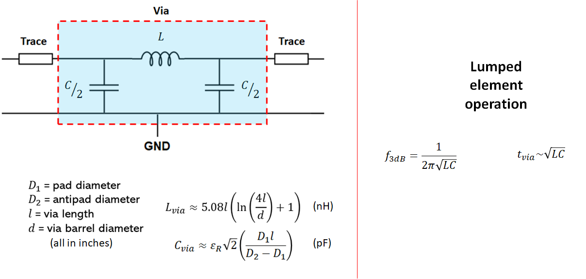
If you use some back-of-the-envelope calculations, you'll find that the via delay on a standard thickness board in the lumped element regime is an order of magnitude approximation of about 40 ps. A more accurate field solver will give about 20 ps propagation delay when no stitching vias are present. Is this an inconsequential number? When do we really need to consider this value?
Do You Need Single-Ended Via Delay?
Why do high-speed designers focus less on via delay than on pin-package delay? There are a few reasons for this:
- High-speed interfaces are mostly differential, and ideally, it's preferred to route both traces in the pair on the same layer. So even if you make layer transitions, you would not create additional total jitter because both signals in the pair experience the same delay.
- Suppose you need to route a differential pair across the entire stackup. If you route into a via to hit an internal layer with one trace, you will have to route through another via to reach the other surface. At some point, you will still have to route the other trace in your differential pair across the stackup as well, incuring the same delay. This effectively eliminates the via skew.
- The above pi filter model with antipads is inherently band-limited, so it is only useful up to a certain bandwidth limit defined by the via's total inductance and capacitance. Howard Johnson discusses this in terms of a rise time limit (e.g., RC circuit) in his textbook, but this would be equivalent to having a 3 dB bandwidth as defined by a typical RC time constant.
Taken together, all these facts mean that the only time you need to worry about via delay is on a wide parallel bus that might have to be routed on an external layer and an internal layer. DDR is a perfect example of this type of interface, and if you split the ADDR/data/strobe/CLK signals into different layers, then you may need to account for the via delay as part of length tuning.
Other buses (either parallel or rather serial buses with a source-synchronous clock) are simply too slow to worry about the need for via delay. SPI and I2C are great examples: even in the fastest cases, the rise time is still a factor 50-100 larger than the delay you would find on a typical via. Therefore, you don't really need to worry about it.
A Special Case Where Single-Ended Via Delay Matters
There is one area where the single-ended via delay matters significantly: RF PCB design and routing. When you're designing an RF system that requires a reference oscillator, and your system is sensitive to the phase of the reference oscillator, then you absolutely must account for via delay and pin-package delay. In this case, you may also need to account for thinks like backdrilling and losses (S11 and S21) of the via as a signal approaches. This type of requirement arises in MIMO systems with phased arrays, or rather any type of cascaded system where there may be multiple transceivers orchestrating send and receive channels in a design.
By default, most PCB design programs with length matching capabilities will set the pin-package delay to zero length or zero time. If you obtain component models from your manufacturer, the IBIS 6 documentation for the particular component should include the pin-package delay. This will be specified as either a length or time. When you include these delays for each component pin in your schematic, you now have the information you need for ultra-accurate length tuning or delay tuning as you route your traces.
The industry-standard design tools in Altium Designer® allow you to specify the pin-package delay for a component directly from your component properties, and the routing engine will automatically include this when applying length matching sections in your PCB layout. Once you’ve completed your PCB and you’re ready to share your high-speed PCB design with collaborators or your manufacturer, you can share your completed designs through the Altium 365™ platform. Everything you need to design and produce advanced electronics can be found in one software package.
We have only scratched the surface of what is possible to do with Altium Designer on Altium 365. Start your free trial of Altium Designer + Altium 365 today.

About Author
Related Resources


Related Technical Documentation


Take advantage of the world's
most trusted PCB design system.
One interface. One data
model. Endless possibilities.
Effortlessly collaborate with
mechanical designers.
The world's most trusted
PCB design platform
Best in class interactive
routing
View License Options
Thank you, you are now subscribed to updates.