With RF Circuit Impedance in Mind Your Designs Won't Look Bird-Brained
Table of Contents
Several years ago, scientists compared the aerodynamic characteristics of several bird species with different species of bats. Feathered bird wings become inactive during the upstroke and maintain lift. Every downstroke increases thrust, lift, and flight speed. In contrast, bats have membranous wings that produce lift during the upstroke. Regardless of their methods, birds and bats overcome weight and drag to achieve flight efficiency.
Two different wing designs and two different flight methods produce the lift-to-weight and lift-to-drag ratios needed for flight. Each amount of wing, body, and induced drag produces an energy cost. Certain characteristics—such as body shape—impact the energy costs for bats. Because wing actions generate less lift, bats fly slower and at shorter distances than birds.
Similarly, a PCB, regardless of its design, will have to work toward its energy needs. There are several characteristics which may lead to impedance within a circuit that a board may maintain. There are many impedances that you may run into. Some of which may be: characteristic impedance, antenna impedance, load impedance or impedance matching. It is your job to understand what may cause these drags and keep your design from lifting up and flying high.
Don’t Let Resistance, Reactance and Impedance Drag You Down
Energy costs in PCB design increase because of the effect of resistance, reactance, and impedance. Resistance opposes a steady electric current. Resistive power results in an energy cost.
Reactance measures the opposition to AC electricity caused by a capacitance or an inductance with reactive power storing energy in electrical and magnetic fields. While a perfect resistance does not vary with frequency, the impact of changing frequencies on a capacitor or an inductor causes reactance to change with frequency.
At this point, the impact of the relationships between reactance, impedance, and frequency on PCB design become more apparent. The impedance of a capacitor has an inverse proportional relationship to capacitance while the impedance of an inductor has a direct relationship with inductance.
RF Circuit Impedance: My, What Large Ears You Have!
The very part that makes a bat special—protruding ears—increases the parasitic drag that reduces energy. Impedance—if not treated correctly—has a dramatic impact on circuit performance. You can impact impedance by working with the thickness and width of trace conductors, the thickness of the dielectric substrate, and the dielectric constant of the substrate impact impedance.
Sudden changes in trace direction can cause changes in impedance. Dielectric constant can change across the length or width of a PCB. Changes in frequency and temperature also cause the dielectric constant to change. Each variance affects the characteristic impedance of an RF circuit.
You’ll need to keep careful track of the sources for impedance in your circuit.
Treating impedance correctly involves several key points. 50-Ω impedance represents the sweet spot for efficient signal transfer. If you achieve a characteristic impedance of 50-Ω in your circuit design, RF signal power transfers efficiently from the source to the load. Few signal reflections occur.
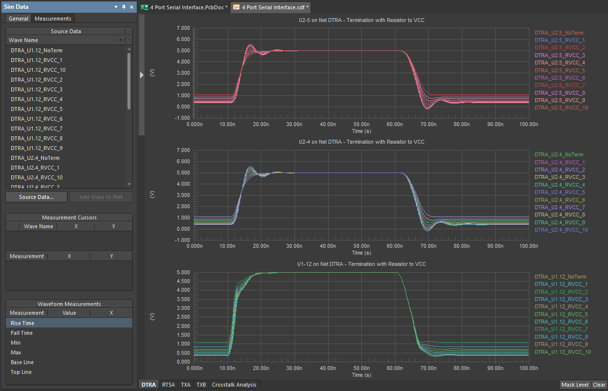
In high-frequency circuits, mismatched impedances between the source and the load harm performance. Reflections and standing waves in high-frequency lines blend with desired signal generator and distort both amplitude and phase.
As the distance from source to load increases, standing waves also cause impedance to ebb and flow. Varying values of impedance can exist because of trace design or the materials used in the trace. If the variances increase, the changes in impedance can lower signal gain, generate noise, or cause random errors.
Say Hello to Controlled Impedance
Judging the flight performance of a bird or bat becomes a matter of perspective. Birds may need to migrate farther and cannot afford to have energy costs take away from speed or endurance. Bats may fly slower but use other tools to locate food.
Digital circuits deliver desired performance because of short transition times and high-clock rates. Devices and appliances have better capabilities because of the faster, sequential transfer of signals. Constantly increasing signal switching speeds requires another look at controlling the impedance of the transmission lines/PCB traces.
Because of transmission line factors, PCB designs require strict values and tolerances for traces. You should use good PCB design techniques to achieve a 50 Ω impedance at transmission line junctions, component connections, and terminators. Matching the impedances (through a matching network) throughout the circuit yields a desired low voltage standing wave ratio (VSWR). Circuits with a low VSWR transfer the maximum power from the source to the load.
Ensure that your designs are working as intended by following design best practices.
I use careful planning to achieve matched impedances within complex RF circuit designs that have broad operating frequencies. Good PCB design software enables me to work with these complex designs (and results, with a smith chart) with ease by giving me the tools necessary to succeed and having an intuitive interface in which to use them.
A strong choice for software, Altium Designer® has tools like a Signal Integrity analysis engine which allows you to match component impedances and use routing to control impedances. As well as use the software to select the signal and plane layer order, the thickness of the copper and dielectric, and the dielectric constant.
If you’d like to consult more about circuit impedance, consider talking to an expert at Altium Designer to learn more.


