Should You Use Thick or Thin FR4 for Your PCB Substrate?

Table of Contents
If you’ve ever made a pie with your kids, you know that the thickness of your crust is important. Too thin, and the pie falls apart into a mess of filling. Too thick, and you might as well be chewing on a loaf of bread. Getting the thickness just right is what makes a pie worth eating.
Even though PCB substrate materials are non-conductive and do not carry current, the thickness of your FR4 PCB substrate determines the board's structural strength, but it also affects power and signal integrity. Your job as a designer is to combine the right set of laminates for the stackup so that the board has the desired thickness, and you won't be able to reach any thickness you want in your PCB. If you're unsure what thickness you should use in your board and just how thick or thin you can get, read these guidelines on FR4 thickness.
FR4 Thickness Design Considerations
The standard thickness of PCBs is 1.57 mm. Some manufacturers will accommodate other specific thicknesses of 0.78 mm or 2.36mm. When we say "thick" or "thin" FR4, we're generally comparing to the standard thickness of 1.57 mm. As long as your manufacturer's process can handle it, you can choose any thickness you like for your PCBs by combining available core and prepreg laminate thicknesses in your PCB stackup.
Before you start selecting laminates and designing your layer stackup, think about the following aspects of your design that are related to board thickness:
Form Factor
Does your PCB have a strict form factor requirement, or does it need to fit into a very slim enclosure? Some designs require a thicker board to support heavier components, withstand mechanically rough environments, or fit into their mechanical supports (high speed backplanes for military and aerospace embedded systems are one example). These constraints can limit your board thickness to specific values.
Components and Edge Connections
Will the device have any components that require the printed circuit board to have a specific PCB thickness? Components like edge connectors and bulkier through-hole components like high current transformers require the PCB stackup have the correct thickness. Some component datasheets and application notes may state a minimum PCB thickness for a specific component for a variety of reasons, and these should be considered when designing the PCB stackup.
An example component where this is important is an SMA edge connector, which is shown below. In this connector, the top and bottom spokes on the connector body are designed to accommodate ~60-70 mil thick PCBs. You can't go above this value if you want to use this specific type of connector, in which case you would have to use a hole-mounted style of SMA. You can go below this value, but then you lose some of the mechanical strength associated with this style of edge connector, which is one of its main benefits.

SMAs are one of the best known styles of edge connectors, but there are other styles that mount to the edge as surface-mount devices, or they use a routed cutout that allows press-fit mounting. Probably one of the most common connectors in the world, USB connectors, are a prime example of the latter type of connector that relies on a specific PCB thickness.
The image below shows a PCB footprint for a USB connector with its routed holes shown for mounting. These holes are standardized and will be shown in the mechanical drawing for a USB connector mounted to the edge of a PCB. The tabs that fit through these holes will help hold the component in place along the edge of the PCB.

The final type of edge-mount connection that can be used in a PCB is with gold fingers along the edge of the PCB. These boards will mount to a slot connector that makes contact with the gold fingers along the board edge, and these connectors require the total board thickness to sit within a specific range. Most designers will be familiar with the gold fingers along RAM modules, PCIe cards, daughtercards, solid-state drives, and key slot connectors.
Trace Impedance
The distance between a trace and its nearest reference plane (on an adjacent layer) determines the trace impedance, as well as the level of dielectric losses in multilayer boards. Going with a thinner layer thickness requires thinner traces. If you want to design to a specific trace width, such as to accommodate a specific connector or IC package, then you should consider the required layer thickness to support the desired width.
It may happen that the layer thickness you need will not end up changing the board thickness, but this depends on the available core and prepreg laminate thicknesses. It's best to check with your fabrication house as to what laminates they have available and design around those laminate thicknesses, rather than set a specific thickness in your design and expect that thickness to be manufacturable.
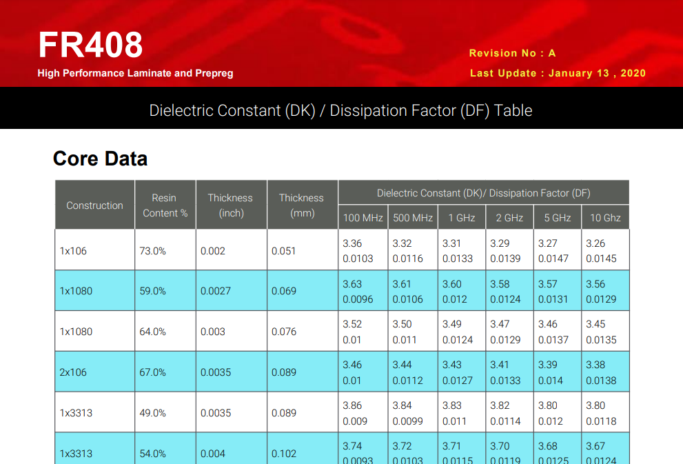
The caveat to this is if you can access a product listing from the laminate manufacturer. Some laminate producers will provide a long list of their available cores and prepregs that include thickness values. As long as you clear it with your fabrication house, you can certainly pick and choose from these lists to propose your own stackup. Just make sure your fabricator stocks the materials and has the processing capabilities needed to support you in this approach. An example list you might find from a laminate vendor is shown below; this list shows a cross-section of core and prepreg data for FR408 materials from Isola.
High-speed/High-frequency PCBs
If you are working with a high-speed device, FR4 is always not the best option, and some other low-loss material may be desirable. If the link length is short, then losses will be dominated by return loss at the load component, so specialty low-loss laminates are not so important. For longer links, the total loss will be dominated by insertion loss, so using a laminate with the lowest loss will help maximize the link length.
Accounting for these points requires considering the same points as in trace impedance. The layer thickness is more important than the total board thickness, but the total board thickness will still be determined by your combination of layers. If you plan to go with thick or thin laminates, think about how layer thickness affects losses. For high speed microstrips, a thicker dielectric layer will confine more field lines in the substrate, thus losses will be greater.
Thermal Expansion, Via Aspect Ratio, and Manufacturability
The next place to consider board thickness is in terms of manufacturability and reliability, specifically in regard to thermal expansion and vias. All materials will expand as they heat up to higher temperatures, including vias in a PCB. In particular, this is important for through-hole vias, which need to be drilled completely through the layer stack. Depending on the board thickness and hole size, you have two tradeoffs to consider when sizing vias:
- Larger aspect ratios can be tougher to plate, and a thicker board will have larger aspect ratio for a given hole size
- A larger hole size is easier to drill and plate, even if the board is thicker
- If the board is too thick, you could increase costs in high volume due to tool wear
- The manufacturer could change the throwing strength in the pulsed plating process to accommodate for high aspect ratio
Through-hole vias with high aspect ratios (10:1 or greater) are susceptible to failure under thermal cycling near the center of the via barrel due to thermal expansion if they are not plated correctly. The manufacturer you use should have experience working with high aspect ratio vias in their fabrication process to ensure you will have a reliable PCB that does not fail under thermal cycling. Before sending out a thick board, make sure they have the capabilities to produce your vias with sufficient wall plating in order to prevent failure.
Obviously, there are a number of design tradeoffs that must be considered when selecting the PCB thickness of an FR4 board, the standard PCB thickness of the layers, and the laminate material. The CAD tools and rules checking features in Altium Designer® make it easy to design your device around the standard FR4 thickness. To learn more, talk to an expert at Altium Designer today.

About Author
Related Resources


Related Technical Documentation


Take advantage of the world's
most trusted PCB design system.
One interface. One data
model. Endless possibilities.
Effortlessly collaborate with
mechanical designers.
The world's most trusted
PCB design platform
Best in class interactive
routing
View License Options
Thank you, you are now subscribed to updates.