Successful PCB Design Data Management
Table of Contents

Previously, we looked at what a successful Data Management system entails and how we would identify a reliable System that is safe to use.
In this blog, we’ll look at what your Data Management system will need to ensure its success. While every Data Management System is unique, there are universal principles which we’ll explore that are vital to a PCB’s utility. These principles are like pillars supporting a bridge; if any single pillar is removed, the others will quickly collapse.
S. Singularity
Singularity is the first principle of PCB Data Management system you’ll need to be successful.
Regardless of the size of your design team, it doesn’t take a psychic to predict the results when your team members are working from different data as their starting points. There just isn’t any way to control the outcome, so it’s not a productive way to operate.
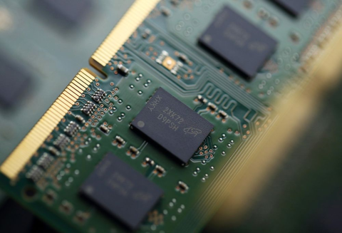
I have seen, time and time again, the problems directly caused by what I call “Rogue Libraries.” Rogue Libraries are libraries of components that are not managed, verified or controlled. Consider the massive amount of work necessary to prepare a PCB design -the engineering, layout, and fabrication process -and then as you get into Assembly the notorious unwanted phone calls begin. Calls letting you know that the assembly house was hitting “snags.” These problems could be anything ranging from parts not going onto the PCB because of wrong footprints, or incorrect decals or pad stacks as they are sometimes called, to component tombstoning or falling off entirely when you start to investigate the initial problem, all just to find that someone used their own personal “Rogue Library.” Use of a Rogue Library usually results in a fatal error for the PCB design and the subsequent scrapping of the entire fabrication. At this point, you’ll take that long walk to the management office to explain the situation. That’s never a good feeling. Rogue Libraries can result in lost profit for the company.
M. Managed
Well, the “official” definition of managed is to be responsible for controlling or organizing someone or something. I am not sure which is worse, to have multiple libraries or having a single library which is unmanaged. They have the same result of producing a bad PCB Design.
In this managed area, there are four areas of concern, revision, lifecycle, roles, and permissions.
Each one of these compliments the other and must be in place to have any success. To pull one causes the collapse of the others and ultimately the collapse of your Data Management System.
A. Architecture
The architecture of the Data Management is most important. The actual building of the structure should have– as we saw in Part-One–the ability to find a specific component and quickly expand. This can be accomplished by organizing your components under a category/Family set up. To use a building-constructon analogy, the further you go into the development stages, the harder it is to reverse course and start over. Often that means merely hitting the delete button and trying it over. This is something that’s happened to me personally, and we had a couple of false starts before we nailed down a system that worked for us.
R. Reliability
The review process–like all the other discussions in this blog–is vital to the success of a PCB Data Management System.
There are two significant categories of the Review process. They are Verification and Validation.
For any verification process to be successful, we must establish and base it on a known standard. What do I mean by standard? It is the benchmark to which we will line up the data. These Verification reports include the component Datasheet and IPC Standards.
Best design practices include quarantining all new components and assuring that they are not used on new PCB designs until they have been reviewed and verified. It may sound like a no-brainer but I have seen the review process in place many times. Use a separate folder which quarantines all new components. Until you finish the audit, those components should not be trusted or used in released designs. The old quote “Trust but Verify” is so vital. Err on the side of caution and attempt to make no assumptions in the design process.
T. Traceability
At this point in the structure of our library, we cross a significant milestone– meaning what we now have is a very stable, and more importantly, reliable library. We can use the data safely. For that reason, many do not go beyond the review process. The tailoring process is a refining procedure of continually improving the information we now have.
When the library begins the tailoring (refining) process, the reports, as we will see, are not just for the library alone. It is a combination of the parts used and the PCB layout. Those reports must be evaluated to determine if the problem is related to a library or a layout issue. That will require conducting a root cause analysis on the data in those reports. There are the initial reports that you should include in PCB fabrication Reports, Design for Manufacturing Reports (DFM), Assembly build findings reports and even the field service Failure reports. All these resources need to be considered to determine the root cause of the problem.
Conclusion
There are endless pitfalls that every PCB designer faces, but with the correct measures in place, you will be able to protect yourself. We are now working in a business environment that has a “take no prisoner” mentality. I will conclude by saying; protect the PCB Data that you use. It represents money to every company–either a profit or a loss. The company succeeds when your PCB Designs succeed, and that’s what happens when you use sound and reliable source of information.
Would you like to find out more about how Altium can help you achieve successful library management? Talk to an expert at Altium and learn more about managing components with ease and confidence.
About Author
Related Resources


Related Technical Documentation

Take advantage of the world's
most trusted PCB design system.
One interface. One data
model. Endless possibilities.
Effortlessly collaborate with
mechanical designers.
The world's most trusted
PCB design platform
Best in class interactive
routing
View License Options
Thank you, you are now subscribed to updates.