What is ESD and How Does it Affect My PCB Design?

Table of Contents
Some environments admit accumulation of static charge, and you won't know it has happened until you receive an annoying shock. While not necessarily harmful to humans when it occurs, it can be harmful to your electronics. Damage can be relatively minor or suppressed when a component is protected, but even weak ESD events are a real danger to electronics that can lead to device failure.
Nearly every conductive element in your PCB layout (traces, routing, electronic component placement) can affect the level of ESD protection on your PCB, and these elements can receive ESD when touched or when exposed to the environment. If you design includes certain interfaces or it must comply with specific ESD withstand voltage requirements, then you will need to consider ESD protection circuits early in your design process.
What is Electrostatic Discharge (ESD)?
Electrostatic discharge (ESD) occurs when two objects with different charges get close enough, or charged enough, to break down (ionize) the dielectric between them. For consumer products, ESD and dielectric breakdown in air usually occurs when the electric field between two points is greater than 40 kV/cm. Things like air pressure, temperature, and humidity will affect this electric field strength. For example, high humidity in some environments can cause the air to be more conductive, which will dissipate some charge and increase the voltage required to create an ESD event.
A typical graph that shows an ESD test pulse is shown below. This test pulse is intended to mimic an ESD event that might occur in practice. The important point in this graph is to notice the rise time and duration of the test pulse. The rise time of real ESD events tends to be very fast, so whatever mechanism you use to protect a circuit, the component needs to respond quickly or else the pulse will impact the load component.

One common misconception is that a specific voltage is needed to cause ESD. This is not exactly correct; the voltage required to produce ESD is dependent on the voltage difference between two points and the distance between those points. This is why, in PCBs, we have a limits on the clearance between conductors (creepage and clearance) as specified in the IPC-2221 standards.
There are other types of transient voltage events that occur, each with different expected peak voltage and peak current levels. The most important difference among the various options for suppressing transient voltages is their response time; this is outlined more in a later section.
How Does ESD Affect a PCB?
Any printed circuit board may be subject to an ESD if it’s touched or comes close enough to people, packaging, cables, or any other object that might produce a large potential difference. When this voltage difference is large enough, there will be a conductive path for current, creating a massive current pulse. As the current pulse develops, high heat is dissipated within the components and the conductors on the PCB itself. At extreme field strengths and developed currents, the PCB can be damaged and components can be destroyed.
This heat dissipation is basically IR drop, where the natural DC resistance of elements in the PCB create a voltage drop and reach high temperature. ESD can occur in some common locations on a PCB, so ESD protection in a PCB should be focused in some particular areas.
ESD in Integrated Circuits
The ESD pulse can cause the path followed by current to flow through the die on an integrated circuit, creating high heat that destroys a component. An example on an integrated circuit package and traces on the semiconductor die are shown below.
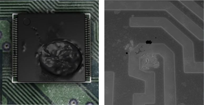
In particular, many modern chipsets are made using such small lithography features that they have little or no tolerance for a high voltage drop, even for DC values slightly above their operating voltage (3.3V or less). The result of an ESD event directly reaching one of these electronic components is usually disastrous, completely ruining the IC and producing the kind of damage shown in the right panel above.
ESD in Connectors
Connectors themselves are not sources of ESD, but any static charge that might build up on or near them can result in an ESD event. Every time someone plugs something in pulls a cable out, or pushes a button, they’re introducing static risk to the device. There is the potential for floating pins to create an ESD event due to static charge handing on the floating conductor. Finally, there is the potential that an ESD event occurs as the connector is plugged into its receptacle, creating a visible spark.

The simple solution for dealing with floating pins is to ground them. Shielded connectors also have metal shielding that can be connected to a grounding point (ideally the chassis) and, eventually, an earth ground connection. Both steps will dissipate any discharge current back to ground and away from any protected circuits. This should be a direct low-reactance connection that immediately to the chassis; don't provide this connection through a capacitor, and don't route an ESD current through the PCB's system ground back to chassis/earth ground.
Implementing ESD Protection on a PCB
The goal in implementing ESD protection on a PCB is to prevent an ESD current from flowing into your circuits and instead divert it into ground through a low-reactance connection. However, in normal conditions, the component still needs to be invisible to any signals traveling along the protected line. The ESD protection circuit or component should only respond when an ESD event occurs, and it must do this very quickly in order to divert the ESD pulse within its rise time.
In general, it is best to drop the ESD pulse to a ground in the system. The best options, arranged in order of priority, are:
- A chassis ground connected to earth
- A chassis connected to system ground, where the connection point is away from the point where ESD is likely to occur
- A guard ring on the PCB, which has the same system ground connection as in #2
- The system ground
The best case is to have the ground off the PCB, which is why chassis grounds are preferred for ESD protection and as a place to dump current in the event of a fault.
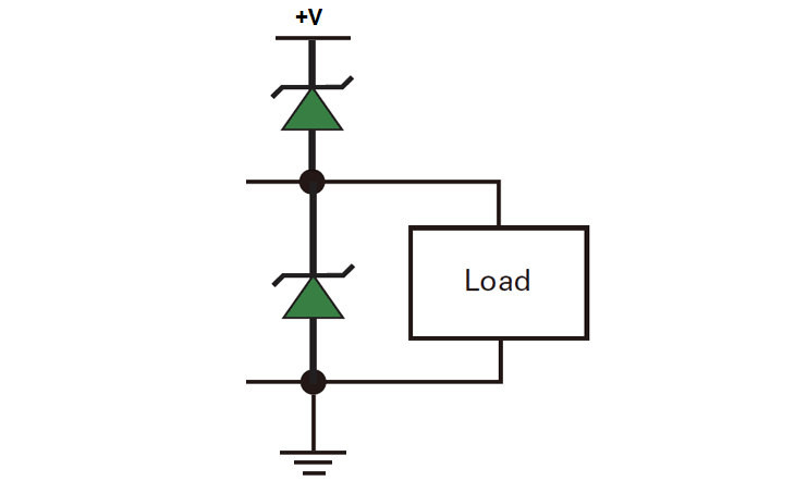
One type of circuit used on the I/Os of some ICs placed near potential ESD sources (like a connector) is a Zener diode (transient voltage suppressor). This small circuit uses 4 Zener diodes that are reverse biased during an ESD event, creating a shunt connection for the ESD voltage/current and protecting the load component. This should be placed very close to the source so that current can be immediately shunted to ground.
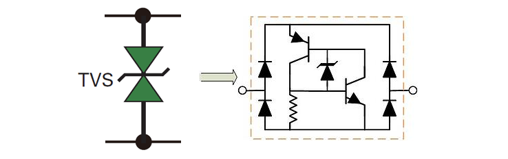
Another option is a TVS diode, which is the other common method for implementing ESD protection on important interfaces. Although we call this component a diode, it is more than just a simple diode, as shown in the equivalent circuit below.
Other ESD protection devices include gas discharge tubes and simple varistors. Discharge tubes are typically marketed for power surges (such as Littelfuse components), rather than for fast ESD events. Make sure you inspect datasheets and understand the response time for the component before using it for ESD protection.
ESD protection for USB, Ethernet, I2C, RS-485, RS-232, and other digital interfaces will generally use a TVS diode between a connector and the IC containing that interface. This is in addition to shielding any metal connector shrouds and unused pins. Your component datasheets will often have some guidelines you should follow to ensure ESD protection. Some companies will also list specific ESD ratings in the datasheets, which might comply with specific industry standards (e.g., automotive or telecom standards), and you might opt for these components when you're designing equipment that might be prone to ESD exposure.
With the best PCB design tools in Altium Designer®, you can implement ESD protection in your PCB, enclosure, and other areas of your electronics to ensure they stay protected. When you’ve finished your design, and you want to release files to your manufacturer, the Altium 365™ platform makes it easy to collaborate and share your projects. We have only scratched the surface of what is possible to do with Altium Designer on Altium 365. You can check the product page for a more in-depth feature description or one of the On-Demand Webinars.

About Author
Related Resources


Related Technical Documentation


Take advantage of the world's
most trusted PCB design system.
One interface. One data
model. Endless possibilities.
Effortlessly collaborate with
mechanical designers.
The world's most trusted
PCB design platform
Best in class interactive
routing
View License Options
Thank you, you are now subscribed to updates.